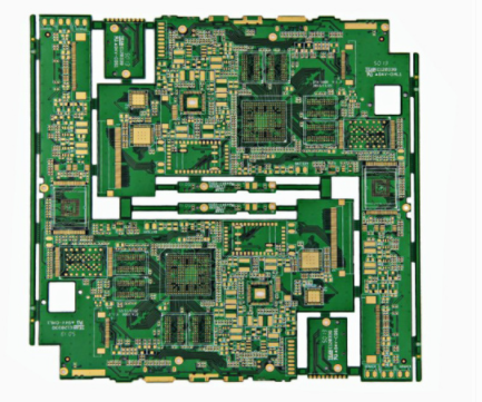
The history of the circuit board
The original name of the circuit board comes from the English PCB (Printed Circuit Board), while the Chinese is translated as "Printed Circuit Board". Some people also call it PWB (Printed Wiring Board). As the name implies, this product is a circuit product made by printing technology. . He replaced the copper wire distribution method for electrical products before the 1940s, which accelerated mass production replication, reduced product volume, increased convenience, and lowered unit prices.
The most advanced circuit board is to melt the metal to cover the surface of the insulating board to make the required circuit. After 1936, the production method has shifted to selecting areas of insulating substrates covered with metal using corrosion-resistant inks, and removing unnecessary areas by etching. This method is called (Subtractive Method).
After 1960, the product market of record players, tape recorders, and video recorders successively adopted double-sided through-hole circuit board manufacturing technology, so the heat-resistant and stable size epoxy resin substrate was widely used, and it is still the main resin for circuit board production. Substrate.

With the evolution of semiconductor technology, electronic products are moving towards higher density structures. Electronic assembly is a one-to-one combination structure. When the density of electronic components increases, of course, the carrier circuit board of the component will also need to increase the connection density, which has gradually formed the design trend of today's high-density circuit board.
Although the concept of build-up circuit boards has appeared in products successively since 1967, it was not until IBM released SLC technology in 1990 that microvia technology gradually became mature and practical. Prior to this, if the full-board through holes of the circuit board were not used, the designer would use multiple pressing methods to obtain a higher wiring density. Due to the rapid advancement of materials, photosensitive and non-photosensitive insulating materials have been listed one after another, and the micro-hole Technology has gradually become the main design structure of high-density circuit boards and appears in many mobile electronic products.
In the connection between circuit layers, in addition to electroplating, the use of conductive paste technology for connectors has also appeared one after another. The more well-known ones are the ALIVH method published by Panasonic and the B2it method published by Toshiba. These technologies are applied to circuit boards. Into the era of high density (High Density Interconnection-HDI).