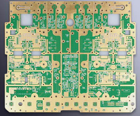
Shenzhen eight-layer circuit board manufacturer
High-precision eight-layer circuit boards are now one of the mainstream products in printed circuit boards, because their wiring density is much higher than that of single-sided PCB circuit boards, and electronic components can be installed on both sides, making the structure of electronic products more reasonable Therefore, as soon as it appeared, it quickly replaced the single-sided circuit board and became the basic unit product for the development of PCB multi-layer boards. The technology is mature and the technology is more complicated. Eight-layer PCB circuit boards can provide high-efficiency and high-quality single-sided PCB circuit boards, double-sided circuit boards, and high-precision eight-layer circuit board manufacturers.
Eight-layer circuit board wiring method:
Generally speaking, the eight-layer PCB circuit board can be divided into the top layer, the bottom layer and two middle layers. The top and bottom layers are connected to the signal lines. The middle layer first uses ADDPLANE to add INTERNALPLANE1 and INTERNALPLANE2 through the command DESIGN/LAYERSTACKMANAGER as the most used power layer such as VCC and ground layer such as GND (that is, connect the corresponding network label. (Be careful not to use ADDLAYER), This will increase the MIDPLAYER, which is mainly used for multi-layer signal line placement), so that PLNNE1 and PLANE2 are two layers of copper connecting the power supply VCC and the ground GND.

If the copper skin is not laid flat, it will crease. The thinner the copper skin of the PCB multilayer board is used, the higher the chance of crease. The thicker copper skin will produce a compression effect and reduce the chance of crease. If it has been confirmed that the copper skin is flat during operation, it depends on whether it is a blank area of the substrate. If the film produces a lot of flow during the melting process, the copper sheet may have poor support and slip. Therefore, most circuit board manufacturers will pay attention to the wiring configuration of the inner substrate, and try to avoid making the empty area excessively obvious. Most of the copper skin creases will occur in areas with large differences in line density, especially where there is a large empty area on one side of the design as a large copper surface.
In addition, the combination method of the film (PP) and the hot pressing parameters are also very important. If the film overlaps and moves or produces improper glue flow, the copper skin will drift on the surface of the molten resin and creases will inevitably occur. To prevent this kind of problem from occurring, the carrier plate used for the pressure plate is the focus of the operation. At present, most of the carrier plate designs used by the industry have adopted the elastic and highly adjustable sliding block design. This design can completely prevent the steel plate from slipping during the pressing process, so that the resulting crease will not occur.
In terms of film selection, try not to use the type with excessive glue content as far as possible, and also adopt a lower level in the pressing and heating rate, as long as the filling can be completed. If the produced PCB circuit board has wrinkles, in the case of loose product specifications, you can consider removing the surface copper and making the press again. Although the board thickness will be slightly higher, if the customer's specifications can be accepted, it can still be remedied.
The following editor will share the processing flow of the high-precision eight-layer circuit board:
Eight-layer copper-clad board blanking, drilling benchmark holes, CNC drilling via holes, inspection, deburring, brushing, electroless plating (through hole metallization), electroplating of thin copper on the whole board, inspection, brushing, and screen printing of negative circuit patterns, Curing (dry film or wet film, exposure, development)-inspection, repairing-circuit pattern plating-tin electroplating (anti-corrosive nickel/gold)-removing printing (photosensitive film)-etching copper-stripping tin-cleaning and brushing a screen Soldering resist graphics (sticking photosensitive dry film or wet film, exposure, development, thermal curing, commonly used photosensitive thermal curing green oil) ~ cleaning, drying-screen printing marking character graphics, curing-shape processing, cleaning, drying-electrical communication Break inspection, spray tin or organic solder mask, inspect packaging, and leave the finished product.
There are vias and blind vias above eight layers. Vias are opened from the top layer to the bottom layer. Blind holes are only visible in one of the top or bottom layers, and the other layer is invisible, that is, blind holes. The hole is drilled from the surface, but not through all layers. There is also a buried via, which is a via in the inner layer, and the surface and bottom layers are invisible. The advantage of making buried vias and blind vias is that it can increase the wiring space.