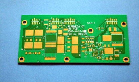
Resin plug hole circuit board manufacturer
In recent years, the resin plugging process has become more and more widely used in the PCB circuit board industry, especially for products with high layers and high-precision PCB multi-layer circuit boards with large thickness. People hope to use resin plug holes to solve a series of problems that cannot be solved by using green oil plug holes or press-fit resin filling. However, due to the characteristics of the resin used in the circuit board process, many difficulties need to be overcome in the manufacture of the circuit board in order to obtain a good quality of resin plugged products. So do you know what the process of resin plugging is? Next, the editor of the circuit board factory will take a look with everyone!
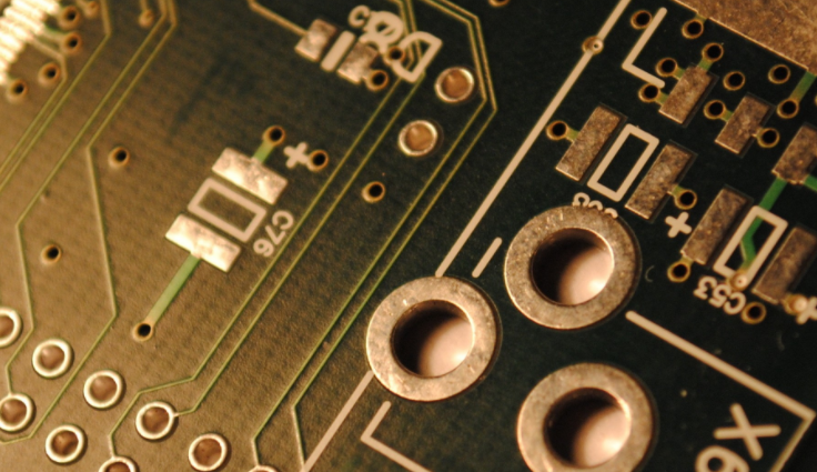
No resin plug hole process on the outer layer of the circuit board
(1) The outer layer is made to meet the requirements of the negative film, and the through-hole thickness-to-diameter ratio is ≤6:1.
The requirements for the negative film of the PCB circuit board are: the line width/line gap is large enough, the maximum PTH hole is less than the maximum sealing capacity of the dry film, and the circuit board thickness is less than the maximum board thickness required by the negative film. And there are no special requirements of the board, the special process board includes: partial electro-gold board, electroplated nickel gold board, half hole board, printed plug board, ringless PTH hole, board with PTH slot and so on.

The production of the inner layer of the circuit board - pressing - browning - laser drilling - debrowning - outer layer drilling - copper immersion - whole board hole filling plating - slice analysis - outer layer pattern - outer layer acid etching - outer layer AOI -Follow-up normal process.
(2) The outer layer is made to meet the requirements of the negative film, and the thickness-to-diameter ratio of the through hole is more than 6:1.
Since the through-hole thickness-to-diameter ratio is greater than 6:1, the use of the entire board for filling and electroplating does not meet the requirements of the copper thickness of the through hole. After the entire board is filled and electroplated, it is necessary to use an ordinary plating line to conduct the through-hole copper Plating to the required thickness, the specific process is as follows:
Inner layer production - pressing - browning - laser drilling - debrowning - outer layer drilling - copper sinking - whole board hole filling plating - full board plating - slice analysis - outer layer graphics - outer layer acid etching - follow-up Normal Process
(3) The outer layer does not meet the requirements of the negative film, the line width/line gap ≥ a, and the thickness-to-diameter ratio of the outer layer through hole ≤ 6:1.
The production of the inner layer of the circuit board - pressing - browning - laser drilling - debrowning - outer layer drilling - copper sinking - whole board hole filling plating - slice analysis - outer layer pattern - pattern plating - outer layer alkaline etching - Outer AOI - Follow-up normal process.
(4) The outer layer does not meet the requirements of the negative film, and the line width/line gap Inner layer production - pressing - browning - laser drilling - debrowning - copper sinking - whole board hole filling electroplating - slice analysis - copper reduction - outer layer drilling - copper sinking (2) - full board electroplating - outer Layer pattern - pattern plating - outer alkaline etching - outer layer AOI - follow-up normal process. iPCB is a high-tech manufacturing enterprise focusing on the development and production of high-precision PCBs. iPCB is happy to be your business partner. Our business goal is to become the most professional prototyping PCB manufacturer in the world. Mainly focus on microwave high frequency PCB, high frequency mixed pressure, ultra-high multi-layer IC testing, from 1+ to 6+ HDI, Anylayer HDI, IC Substrate, IC test board, rigid flexible PCB, ordinary multi-layer FR4 PCB, etc. Products are widely used in industry 4.0, communications, industrial control, digital, power, computers, automobiles, medical, aerospace, instrumentation, Internet of Things and other fields.