Causes of poor tin on lead-free tin-sprayed circuit boards (circuit boards)
The editor of the PCB factory believes that most friends who play the SMT patch process will first doubt whether it is the poor printing of the solder paste (the thickness of the steel mesh, the opening, the pressure Etc.), solder paste over-aging oxidation, SMD component foot oxidation, or reflow soldering temperature profile is not adjusted properly. In fact, there is another reason that cannot be ignored, which is the thickness of the sprayed tin from the sprayed tin circuit board. The thickness of the gold layer and the nickel layer of ENIG that everyone is familiar with before should cause soldering problems. Will the tin layer of the tin circuit board (circuit board) be too thin to cause defective soldering? Below are some collected book data for your reference.
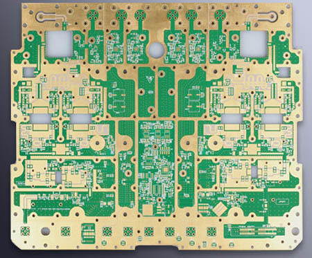
Lead-free spray tin (HASL) top tin bad case
Analyze the cause of poor tin eating after reflow soldering on the second side of the HASL circuit board(circuit board). The results of metallographic section analysis show that the copper-tin alloying phenomenon has appeared where the solder pads are not eaten, and this kind of copper-tin alloy can no longer provide solderability.
Inspecting the empty PCB boards of the same batch without soldering and doing slice analysis, it was found that the soldering pads of the unsoldered circuit boards (circuit boards) had serious alloy exposure in the tin plating layer. The slicing of the blank PCB board can also find the formation of copper-tin alloy. The measured thickness is about 2μm. After considering the alloy will cause the thickness to increase, it is speculated that the original spray tin thickness should be less than 2μm, so the root cause is inferred. The thickness of the sprayed tin is too thin (below 2µm), so that the copper-tin alloying has been exposed to the surface of the solder pad, and there is not enough tin to be combined with the solder paste, which will affect the effect of the solder pad eating tin.
")
How to deal with poor tin on one side of double-sided tin-spray circuit board(circuit board)
This should be a collated article that gathers opinions from all parties, but in the end, it was mostly attributed to the thickness of the sprayed tin being too thin, which resulted in poor soldering.
The spray tin thickness is recommended to be at least 100u” (2.5µm) or more in the large copper area, 200u” (5.0µm) or more in the QFP and peripheral parts, and 450u” (11.4µm) or more in the BGA pad, which can solve the problem. Reflow soldering on both sides will cause solder rejection, but the thicker the spray tin is, the more disadvantageous it is for the parts with fine pins, and the problem of short circuits is likely to be formed.
In the manufacturing process of the PCB board, the smaller the thickness of the solder pad, the thicker it will be, which will easily cause a short circuit to the fine inter-pin parts.
The longer the storage time of the sprayed circuit board(circuit board) is, the thicker the thickness of the IMC (Cu6Sn5) will be, which will be more unfavorable for subsequent reflow soldering. Generally, the flatter the tin of the tin spray board, the thinner the thickness becomes.