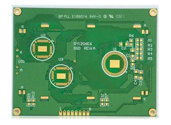
What is the reason for the uneven copper hole of the circuit board?
Shenzhen Circuit Board Factory:Question: What is the cause of uneven copper holes in the circuit board? What are the reasons for UNEVENPLATING (pulse plating is used)? how to improve? Does the amount of current have anything to do with the thickness of the plating and the width of the trace? What is the relationship?
Answer: I don't know whether your electroplating equipment uses a single rectifier or a bilateral control design. If it is a single rectifier control structure, the electroplating current distribution will be directly affected by the contact resistance. If the hole is deep and the uniformity of the liquid medicine flow is not ideal, the problem of uneven thickness of the unilateral hole will occur. In addition, I don't know whether the circuit board you are discussing is full-board plating or line plating. If it is line plating, it can only be said that unevenness is inevitable. The difference lies in what level the full-range can achieve. Pulse electroplating belongs to AC electroplating, which is more sensitive to waveforms. If the contact condition is not ideal, unevenness of the left and right halves may also occur.

The uniformity of electroplating is divided into large areas and small areas. The unevenness of large areas has a higher possibility of improvement, but it is more difficult to improve local areas. Generally, when discussing the problem of uneven plating, the main consideration is the distribution of power lines. For electroplating, the so-called power line is an imaginary travel path formed by charged particles. The factors that affect the distribution of these hypothetical routes include: anode configuration, distance between cathode and anode, circuit board suspension, chemical solution stirring, circuit board swing, current density, gloss system type, shielding system design, etc.
For large areas, appropriate adjustments will help. However, for small areas, especially for line electroplating, because the copper surface distribution has been irregular, and the cathode configuration and design are fixed, the power line distribution will inevitably cause mutual repulsion. Uneven distribution. At present, most effective methods are improved by using a lower current density and proper gloss system. For other mechanical designs, please adjust the equipment manufacturers appropriately. There should be room for improvement.
The magnitude of the current is related to the plating area, which we call current density. The more uniform the current distribution, the better the electroplating quality, and the higher the current density is, the shorter the time for the same copper plating thickness. However, high current density is often accompanied by the problem of poor electrical uniformity. How to balance production and quality is a problem you must think about. Generally speaking, if the line becomes thinner and the copper surface is unevenly distributed, then theoretically it means that the current density that can be used is lower.
When the early circuit board manufacturers faced the problem of electroplating uniformity, another more direct thinking was to increase the distance between the anode and the anode. This treatment can reduce the power line repellency to a relatively low level. It really helps. However, this treatment consumes more energy and is not an appropriate treatment method for pulse electroplating. For circuit electroplating, the dense circuit area will bear more uniform current, but the current distribution in the independent circuit area (sparse and uneven area) will be worse. At this time, if possible, some false points should be added on the circuit board to disperse the current, Otherwise the plating uniformity will inevitably become worse.