1G makes calls, 2G chats with QQ, 3G scans Weibo, 4G watches videos, 5G downloads a movie in one second... I believe this is the understanding of most people's mobile communication technology iteration. As everyone knows, as a new generation of revolutionary technology, the fifth-generation mobile communication technology (5G) not only means a doubled increase in data transmission speed, but also a true convergent network. Related application areas will be promoted, such as the Internet of Things, Applications such as Industry 4.0, artificial intelligence, the Internet of Vehicles, and interactive multimedia will be popularized in large numbers, thus forming an era of "Internet of Everything".
PCB as the "mother of electronic products", profound changes in the downstream consumer market will directly affect the development trajectory of the PCB industry. The industry generally believes that in the next three to five years, 5G communications will surpass today's two major application markets, smart terminals and automotive electronics, and become the number one engine driving the growth of the PCB industry.
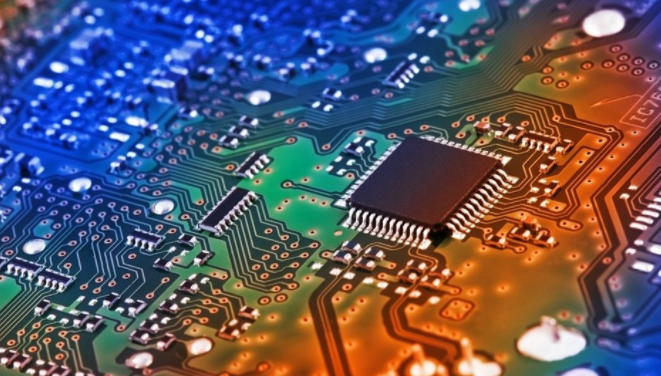
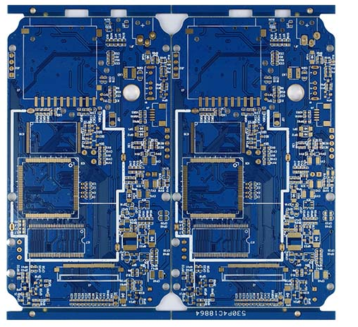
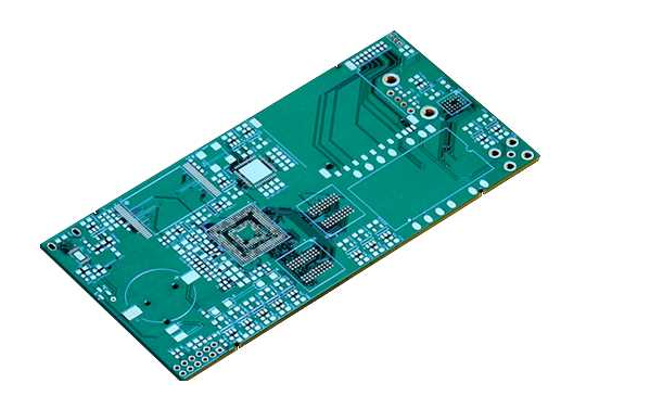
China PCB enters the 5G era
Since 2010, the growth rate of global PCB production value has generally declined. On the one hand, fast-iterative new terminal technologies continue to impact low-end production capacity. Single and double panels, which once ranked first in output value, are gradually being replaced by high-end production capacities such as multilayer boards,HDI, FPC, and rigid-flex boards. On the other hand, the weak terminal market demand and the abnormal price increase of raw materials have also made the entire industry chain turbulent. PCB companies are committed to reshaping their core competitiveness, transforming from "winning by quantity" to "winning by quality" and "winning by technology." ".
What is proud of is that under the background of both the global electronics market and the global PCB output value growth rate, the annual growth rate of China's PCB output value is higher than that of the world, and the proportion of total output value in the world has also increased significantly. Obviously, China has become a global PCB. The largest producer of the industry, China's PCB industry has a better state to welcome the arrival of 5G communications!
Actively optimistic about the 5G PCB market
"In fact, 5G communication has been mentioned for several years, and the real product launch should be in 2019." Wu Yuanli, component procurement manager of Xingsen Technology Purchasing Management Center, said in an interview, "So the current 5G industry chain pattern has not yet formed. Enterprises are all qualified to fight for the right to speak in 5G. It is foreseeable that 5G will mature and develop rapidly in the next three years. This 5G PCB competition must be very exciting!"
Chen Chun, chief engineer of Jinbaize Technology, told reporters: "Since last year, Jinbaize has been testing 5G products for customers, and has already begun to produce some medium-volume 5G orders for some customers." According to reports, Jinbaize Technology is an integrated electronic circuit design service for R&D. With manufacturing service providers, the business includes electronic product hardware design, PCB design, PCB manufacturing, EMS and BOM engineering optimization, etc.
Chen Chun said: "According to relevant industry research data, the annual output value of PCBs for radio frequency side base stations brought by only 5G in the world can reach more than 24 billion yuan per year (Mainland China is expected to account for 50%), which is more than four times that of 4G. Based on the 5G PCB technical specifications, in addition to the needs of the PCB itself, the application of 5G will bring new growth momentum to upstream suppliers such as high-frequency and high-speed materials, more sophisticated production and testing equipment, and new surface treatment processes."
As a well-known PCB design company in China, Yibo Technology estimates the market value of 5G communication to the PCB industry from a design perspective. "The popularity of 5G requires more radio frequency transmission equipment to be deployed in the same area. In other words, a large number of signal radio frequency devices are required to meet 5G data transmission and all-weather coverage of the entire social area. The demand for these equipment is high frequency The processing of plates and high-frequency circuit boards is a huge driving force." said Wu Jun, vice president of research and development of Yibo Technology.

The challenge of 5G communication to PCB technology
5G PCB process technology development direction
Material requirements: A very clear direction for 5G PCB is high-frequency and high-speed materials and board manufacturing. Wu Jun pointed out that in terms of high-frequency materials, it is obvious that leading material manufacturers in traditional high-speed fields such as Lianmao, Shengyi, and Panasonic have begun to deploy high-frequency plates and introduced a series of new materials. This will break the current dominance of Rogers in the field of high-frequency panels. After healthy competition, the performance, convenience and availability of materials will be greatly enhanced. Therefore, the localization of high-frequency materials is an inevitable trend.
In terms of high-speed materials, Wu Yuanli believes that 400G products need to use materials equivalent to M7N and MW4000. In the backplane design, M7N is already the lowest loss option. In the future, backplanes/optical modules with larger capacity will require lower loss materials. The combination of resin, copper foil, and glass cloth will achieve the best balance between electrical performance and cost. In addition, the number of high-levels and high density will also bring reliability challenges.
Requirements for PCB design: The selection of plates must meet the requirements of high-frequency and high-speed, impedance matching, stacking planning, wiring spacing/holes, etc. must meet the signal integrity requirements, which can be from loss, embedment, high-frequency phase /Amplitude, mixed pressure, heat dissipation, PIM these six aspects.
Requirements for process technology: Wu Jun believes that the enhancement of 5G-related application product functions will increase the demand for high-density PCBs, and HDI will also become an important technical field. Multi-level HDI products and even products with any level of interconnection will be popularized, and new technologies such as buried resistance and buried capacitance will also have more and more applications.
Chen Chun added that PCB copper thickness uniformity, line width accuracy, interlayer alignment, interlayer dielectric thickness, control accuracy of back drilling depth, and plasma de-drilling capability are all worthy of in-depth study.
Requirements for equipment and instruments: Wu Yuanli pointed out that high-precision equipment and pre-processing lines with less roughening of the copper surface are currently ideal processing equipment; and the testing equipment includes passive intermodulation testers, flying probe impedance testers, and loss Test equipment, etc.
Chen Chun believes that sophisticated graphics transfer and vacuum etching equipment can monitor and feedback data changes in real-time line width and coupling distance detection equipment; electroplating equipment with good uniformity, high-precision lamination equipment, etc. can also comply with 5G PCB production needs.
Requirements for quality monitoring: Due to the increase of 5G signal rate, the board-making deviation has a greater impact on signal performance, which requires stricter control of the board-making production deviation, while the existing mainstream board-making process and equipment are not updated., Will become the bottleneck of future technological development. How to break the situation for PCB manufacturers is of utmost importance.
In terms of quality monitoring, Jinbaize further strengthens the statistical process control of key product parameters, and manages data in a more real-time manner, so that the consistency of the product can be guaranteed to meet the performance requirements of the antenna in terms of phase, standing wave, and amplitude.
How to control the cost of 5G?
For any new technology, the cost of its initial research and development is huge. Moreover, 5G communication has not been launched for a long time, and "high investment, high return, and high risk" has become the consensus of the industry. How to balance the input-output ratio of new technologies? Local PCB companies have their own abilities in cost control.
Wu Jun believes that there are two ways of cost management. One way is to balance costs through the increase of production scale and capacity, which will form some large-scale production enterprises; Design and development are more flexible, so as to cope with the pressure of fast delivery brought by the shortened product cycle.
Jin Baize, who has the advantages of hardware design and PCB design, believes that the most important thing to reduce costs and increase efficiency is to start from the source. Chen Chun explained that in the PCB engineering design stage, it is necessary to optimize the design around the cost, and convene a cross-departmental team to conduct a special cost review. Through the early participation of the procurement, production, and process departments in the engineering stage, changes are proposed. More cost-reducing design. For example, you can increase the utilization rate by customizing the size of the board and combining products with similar process flows, increasing the size of the production board, and optimizing the laminated structure to reduce the cost of the board.
Different from the first two, the cost control logic of Xingsen Technology has more drastic characteristics. As long as the input and output must be proportional, Xingsen has the confidence to break through. As for its IC substrate business, since its layout in 2013, it has invested more than 1 billion yuan in five years, but it has suffered losses for five consecutive years. Until the second half of 2018, Xingsen Technology finally successfully entered the industrial chain of South Korean Samsung, Kingston, Hynix and other well-known companies, and orders flooded like snowflakes. At present, the company's IC substrate business has been operating at full capacity, and orders are even scheduled for next year.
In the same way, Xingsen Technology will certainly not miss out on the unlimited business opportunities in the 5GPCB market. Wu Yuanli said that on the one hand, the starting point of 5G PCB technology is high, the initial equipment investment is large, and the professionals are lacking. It is difficult for ordinary small and medium-sized enterprises to achieve overnight. Xingsen Technology has always reserved competitive advantages in process technology, supporting equipment, and professional talents. On the other hand, due to the delay of 5G communication products, 5G PCB is essentially a trial production product developed by end customers in a short period of time. This requires PCB companies to synchronize with end customers and equipment manufacturers in an all-round way. Adjust and match customer needs. At present, Xingsen Technology has reached long-term cooperation with global 5G leaders such as Samsung, Huawei, and ZTE, and has obvious customer advantages.
In addition, in order to reduce the double cost of customer procurement and company sales, Xingsen Technology is also continuing to deepen one-stop PCB customization services, from CAD design, sales, manufacturing, SMT surface mounting, and even e-commerce platforms. middle.
Manufacturing PCB in a smarter and environmentally friendly environment
It cannot be denied that PCB is a high-tech industry, but due to the etching and other processes involved in the PCB manufacturing process, PCB companies have unknowingly been misunderstood as "big polluters", "big energy users" and "big water users". Today, when we attach great importance to environmental protection and sustainable development, once PCB companies are put on the "pollution hat", it will be difficult, not to mention the development of 5G technology. Therefore, Chinese PCB companies have built green factories and smart factories one after another.
In terms of environmental protection, the more developed the economy of the area where PCB companies are located, the greater the restrictions and management they are subject to. The three manufacturing plants of Xingsen Technology, Jinbaize Technology, and Yibo Technology are located in Guangzhou, Huizhou, and Shenzhen, respectively. They are located in Guangdong, the most economically developed region in the country. Therefore, when talking about PCB environmental protection work, the three interviewees were deeply moved.
"Energy saving and environmental protection are a hurdle that PCB companies cannot avoid. In addition to investing heavily in promoting energy conservation and emission reduction, Xingsen Technology also regularly communicates with government agencies and environmental protection units to adhere to the national government's environmental protection goals and requirements." Wu Yuanli Said.
In terms of smart factories, due to the complexity of PCB processing procedures and many types of equipment and brands, there is great resistance to the full realization of factory intelligence. At present, the level of intelligence in some newly-built factories is relatively high, and the per capita output value of some advanced and newly-built smart factories in China can reach more than 3 to 4 times the industry average. But others are the transformation and upgrading of old factories. Different communication protocols are involved between different equipment and between new and old equipment, and the progress of intelligent transformation is slow.
According to reports, Xingsen Technology's smart factory transformation project in Guangzhou Science City will be completed by the end of this year. By then, the smart factory will be almost fully automated, and the required staff will be further reduced. It is expected that the output value will be more than three times higher than the original.
"In 2019, Jinbaize is exploring the creation of a digital middle office to connect front-end services and back-end manufacturing systems." Chen Chun introduced, "For Jinbaize, we introduced the concept of intelligent design and manufacturing earlier, because We have the characteristics of flexible manufacturing with many varieties and small batches, so we applied digital direct laser imaging system, smart inkjet printing system and other smart equipment and smart engineering software ten years ago, which is relatively leading in the industry.