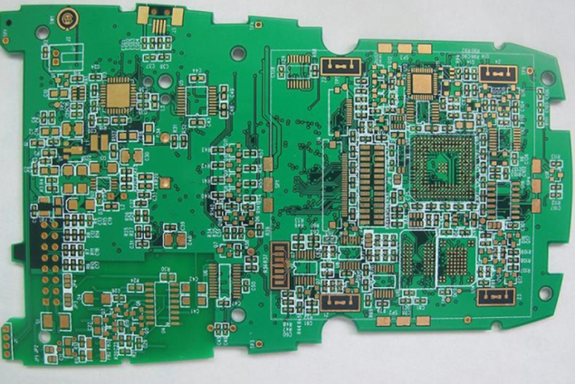
Some defects in the manufacturing process of multilayer circuit boards
1. Circuit distortion caused by poor etching of multilayer circuit boards
When etching the outer circuit of a multilayer circuit board, if the copper foil ridge line penetrates into the resin of the board surface quite deep, residual copper may remain in the dense circuit area after etching. These phenomena may not be easy to detect after etching, but it is not easy to detect after etching. After the nickel immersion gold process, it may be found that the lines or the edges of the solder pads have deformed lines or metal areas. This problem is sometimes regarded as a problem of residual or poor washing, but it is actually a problem of circuit etching or improper copper selection.

Second, the gold and copper that may be caused by poor tin stripping
It is necessary to pay attention to peeling tin after etching to see if there is still light gray intermetallic that has not been stripped. If it is not completely removed, brushing, pickling, and microetching may not be completely removed, which will inhibit the initiation of the nickel immersion gold reaction. If the reaction fails to start at all, copper leakage on the gold-plated surface may occur.
Third, the problem of residual copper on the wall of the copper-free through hole
The current practice of copper-free vias is mainly to perform etching and removal after full copper plating, or to prevent the holes from being plated with tin by a cap hole process, and then etching to remove the copper. However, the etching solution has no way to remove the palladium metal, so the nickel and gold will still be adsorbed on the pore wall during the process. This is a direct problem for these products that do not require metal on the hole wall.
At present, some multi-layer circuit board manufacturers have introduced the so-called chemical copper process that is troubled by nickel-free immersion gold. In fact, the simple method is to reduce the concentration of palladium metal. By this method, the subsequent nickel-gold can not be quickly plated, so it can reduce There is no trouble with the production of copper through holes. However, such an approach will have the potential risk of insufficient chemical copper activity and pore rupture, and the operating range of chemical copper will be reduced. Some manufacturers also use the method of removing palladium, adding a liquid treatment for removing palladium after stripping the tin bath. However, this method must increase the setting of the liquid bath in the current process, and the operating cost will also increase.
At the same time, most palladium removal systems have the risk of corrosion of copper, and some so-called special yao water has patent and cost issues. Another method is to passivate the palladium layer in the hole with a mercaptan solution before stripping the tin, so that the subsequent nickel immersion gold process cannot work. However, if the mercaptan treatment is not clean, the residue will be carried into the tin stripping tank and the copper surface will be stained with sulfide. The sulfur on the copper surface is a fatal injury to the nickel reaction, so it is very difficult to prevent the problem of copper exposure. For this reason, the current exact solution for copper-free vias is still under development.
iPCB is a high-tech manufacturing enterprise focusing on the development and production of high-precision PCBs. iPCB is happy to be your business partner. Our business goal is to become the most professional prototyping PCB manufacturer in the world. Mainly focus on microwave high frequency PCB, high frequency mixed pressure, ultra-high multi-layer IC testing, from 1+ to 6+ HDI, Anylayer HDI, IC Substrate, IC test board, rigid flexible PCB, ordinary multi-layer FR4 PCB, etc. Products are widely used in industry 4.0, communications, industrial control, digital, power, computers, automobiles, medical, aerospace, instrumentation, Internet of Things and other fields.