What is the difference between HDI circuit board and ordinary PCB board
What is the difference between HDI circuit board and ordinary PCB board?
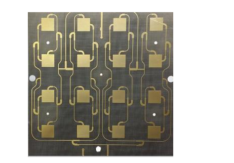
Yes, this is the most basic HDI circuit board. .
It means that both the first layer and the last layer need to be drilled with blind holes (usually done by laser drilling). These holes are mainly drilled in the BGA area. There should be enough space elsewhere.
If it is a four-layer circuit board, it is 1-2 layers and 3-4 layers
If it is a six-layer circuit board, it is 1-2 layers and 5-6 layers
As for the buried-hole circuit board, it can't be seen like this. . It depends on how the specific data engineer designed it.

How to distinguish HDI circuit board PCB first-order, second-order and third-order?
The first-order is relatively simple, and the process and craftsmanship are well controlled.
The second order started to be troublesome, one was the alignment problem, and the other was the problem of punching and copper plating. There are many second-order designs. One is that each step is staggered. When connecting the next adjacent layer, it is connected through a wire in the middle layer, which is equivalent to two first-order HDI circuit boards. The second is that the two first-order holes overlap, and the second-order is achieved by superposition. The processing is similar to two first-order, but there are many process points to be specially controlled, which is mentioned above. The third is to punch directly from the outer layer to the third layer (or N-2 layer). The process is different from the previous one, and the difficulty of punching is also greater.
For the third-order analogy, it is the second-order analogy.
Are PCB boards with blind and buried vias called hdi boards?
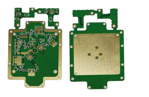
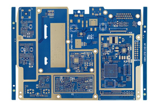
HDI boards are high-density interconnected circuit boards. The boards that are plated with blind holes and then laminated are all HDI boards, which are divided into first-order, second-order, third-order, fourth-order, and fifth-order HDI. For example, the motherboard of iPhone 6 is fifth-order HDI.
A simple buried via is not necessarily an HDI circuit board.
What is the difference between HDI circuit board and traditional PCB board?
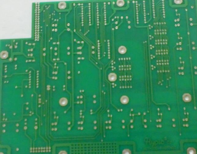
Ordinary PCB circuit boards are mainly FR-4, which is laminated with epoxy resin and electronic grade glass cloth. Generally, traditional HDI circuit boards use back adhesive copper foil on the outermost surface, because laser drilling, Can not get through the glass cloth, so generally use glass fiber-free back adhesive copper foil, but the current high-energy laser drilling machine can penetrate 1180 glass cloth. This is no different from ordinary materials.
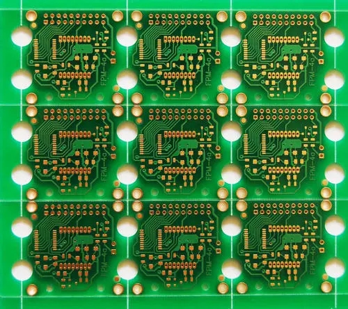
What kind of PCB board is called HDI circuit board? What is the difference between them and ordinary double-sided panels? What's more, the high-frequency board is usually pressed with FR4 glass fiber board, and it is pressed by the entire epoxy glass cloth, the color of the whole board is relatively uniform and bright. The density is greater than that of the low-frequency board. Generally, high-frequency boards are used in circuits with frequencies above 1G. Its dielectric constant is the key, it must be very small and stable, the dielectric loss is small, it is not easy to absorb water and moisture, heat resistance, corrosion resistance and other excellent properties.
HDI circuit board is a high power density inverter (High Density Inverter), a telephone board with a relatively high line distribution density using micro-blind buried via technology. It is a compact product designed for small-capacity users. It adopts modular and parallel design. One module has a capacity of 1000VA (1U height) and is naturally cooled. It can be directly placed in a 19" rack, and up to 6 modules can be connected in parallel. The product adopts all-digital signal process control (DSP) technology and multiple A patented technology, with a full range of adaptable load capacity and strong short-term overload capacity.
Many common printed circuit boards are made of low-end materials, such as paper substrates, composite substrates, epoxy boards (also called 3240 epoxy boards, phenolic boards), and FR-4 fiberglass boards(composite boards). Paper substrate and composite substrate.
What does hdi circuit board mean in the PCB industry?
HDI is the abbreviation of High Density Interconnect, literally translated into high-density interconnection, it actually uses microvias, buried vias, sequential lamination (I don’t know what it translates into, it means sticking a layer of dielectric and a layer of copper foil on the surface of the PCB, and then hitting it. Microvia, etching), which is different from the traditional process of pressing core and prepreg together and then drilling through holes. All of this is for higher wiring density.
What are the first-order and second-order HDI PCB boards?
The first-order board is formed by pressing it once. It can be imagined as the most common board. The second-order board is pressed twice. Take the eight-layer circuit board with blind and buried holes as an example. First make a 2-7 layer board and press it. At this time, the 2-7 through-hole buried holes have been completed, then add 1 layer and 8 layers, and punch 1-8 through holes to make the whole board. The third-order board is more complicated than the above, press 3 first -6 layers, plus 2 and 7 layers, and finally 1 to 8 layers...