What are the methods that PCB manufacturers need to improve when using dry film
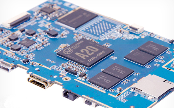
With the rapid development of the electronics industry, the wiring of PCB boards is becoming more and more precise. Many PCB manufacturers use dry film to complete graphics transfer, and the use of dry film is becoming more and more popular. However, in the process of after-sales service, I still I have encountered many misunderstandings in the use of dry film by many customers, and I have summarized them for reference.
1. The PCB board has holes in the dry film mask
Many customers believe that after a hole occurs, the film temperature and pressure should be increased to enhance its bonding force. In fact, this view is incorrect, because the solvent of the resist layer will evaporate excessively after the temperature and pressure are too high, which will cause dryness. The film becomes brittle and thinner, and the holes are easily broken during development. We must always maintain the toughness of the dry film. Therefore, after the holes appear, we can make improvements from the following points:
1. Reduce the temperature and pressure of the film;
2. Improve drilling and piercing;
3. Increase exposure energy;
4. Reduce developing pressure;
5. Do not stretch the dry film too tightly during the pasting process;
6. After sticking the film, the parking time should not be too long, so as not to cause the semi-fluid yao film in the corner to diffuse and thin under the action of pressure.

Second, the PCB board has seepage plating during dry film electroplating
The reason for the permeation is that the dry film and the copper clad board are not firmly bonded, which causes the plating solution to deepen, which causes the "negative phase" part of the plating layer to become thicker. The permeation of most PCB manufacturers is caused by the following points:
1. Exposure energy is too high or low
Under ultraviolet light irradiation, the photoinitiator that has absorbed the light energy decomposes into free radicals to initiate a photopolymerization reaction, forming a body-shaped molecule that is insoluble in a dilute alkali solution. When the exposure is insufficient, due to incomplete polymerization, the film swells and becomes soft during the development process, resulting in unclear lines or even the film layer falling off, resulting in poor bonding between the film and copper; if the exposure is overexposed, it will cause development difficulties and also during the electroplating process. Warping and peeling occurred during the process, forming penetration plating. Therefore, it is very important to control the exposure energy.
2. The film pressure is too high or low
When the film pressure is too low, it may cause uneven film surface or gaps between the dry film and the copper plate and fail to meet the requirements of the bonding force; if the film pressure is too high, the solvent and volatile components of the resist layer will volatilize too much, causing The dry film becomes brittle and will be lifted and peeled after electroplating electric shock.
3. The film temperature is too high or low
If the film temperature is too low, the resist film cannot be sufficiently softened and flowed properly, resulting in poor adhesion between the dry film and the surface of the copper clad laminate; if the temperature is too high, the solvent and other volatility in the resist The rapid volatilization of the substance produces bubbles, and the dry film becomes brittle, causing warping and peeling during electroplating electric shock, resulting in infiltration.
iPCB is a high-tech manufacturing enterprise focusing on the development and production of high-precision PCBs. iPCB is happy to be your business partner. Our business goal is to become the most professional prototyping PCB manufacturer in the world. Mainly focus on microwave high frequency PCB, high frequency mixed pressure, ultra-high multi-layer IC testing, from 1+ to 6+ HDI, Anylayer HDI, IC Substrate, IC test board, rigid flexible PCB, ordinary multi-layer FR4 PCB, etc. Products are widely used in industry 4.0, communications, industrial control, digital, power, computers, automobiles, medical, aerospace, instrumentation, Internet of Things and other fields.