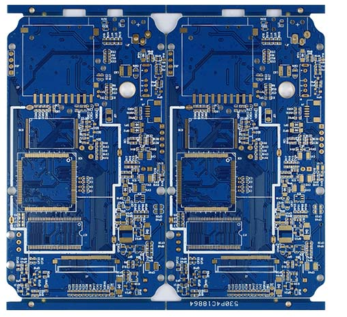
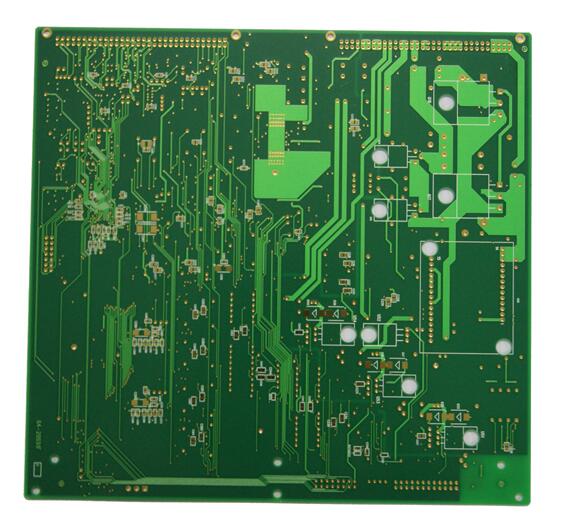
Several common surface treatment methods for PCB board proofing
The surface treatment methods used in PCB proofing are different. Each surface treatment method has its own unique characteristics. Taking chemical silver as an example, its process is extremely simple. It is recommended to use lead-free soldering and smt, especially for fine The circuit effect is better, and the most important thing is to use chemical silver for surface treatment, which will greatly reduce the overall cost and lower cost. The editor of the circuit board factory will introduce you to several common surface treatment methods for PCB board proofing.

1. HASL hot air leveling (that is, spray tin)
Tin spraying is a common processing method in the early stage of PCB proofing. Now it is divided into lead spray tin and lead-free spray tin. The advantages of tin spraying: After the PCB is completed, the copper surface is completely wetted (the tin is completely covered before soldering), suitable for lead-free soldering, the process is mature and the cost is low, suitable for visual inspection and electrical testing, and it is also a high-quality and reliable PCB board One of the proofing processing methods.
2. Chemical nickel gold (ENIG)
Nickel gold is a relatively large-scale PCB proofing surface treatment process. Remember: the nickel layer is a nickel-phosphorus alloy layer. According to the phosphorus content, it is divided into high-phosphorus nickel and medium-phosphorus nickel. The application is different, so we will not introduce it here. the difference. The advantages of nickel gold: suitable for lead-free soldering; very flat surface, suitable for SMT, suitable for electrical testing, suitable for switch contact design, suitable for aluminum wire binding, suitable for thick plates, and strong resistance to environmental attacks.
3. Electroplated nickel gold
Electroplated nickel gold is divided into "hard gold" and "soft gold". Hard gold (such as gold-cobalt alloy) is commonly used on gold fingers (contact connection design), and soft gold is pure gold. Electroplating of nickel and gold is widely used on IC substrates (such as PBGA). It is mainly suitable for bonding gold and copper wires. However, the plating of the IC substrate is suitable. The bonded gold finger area needs to be electroplated with additional conductive wires. The advantages of electroplated nickel-gold PCB board proofing: suitable for contact switch design and gold wire binding; suitable for electrical testing
4. Nickel Palladium (ENEPIG)
Nickel-palladium-gold is now gradually beginning to be applied in the field of PCB proofing, and it has been used more in semiconductors before. Suitable for bonding of gold and aluminum wires. Advantages of proofing with nickel-palladium-gold PCB board: application on IC carrier board, suitable for gold wire bonding and aluminum wire bonding. Suitable for lead-free soldering; compared with ENIG, there is no nickel corrosion (black plate) problem; the cost is cheaper than ENIG and electro-nickel gold, suitable for a variety of surface treatment processes and on-board.
In addition to the above several kinds of PCB proofing treatment methods, it also includes chemical tin. This chemical tin surface treatment is suitable for horizontal line production, and is also used. In fine circuit processing projects, when you choose the PCB proofing surface treatment method, you need to follow According to the actual situation, contact the characteristics of the surface treatment method and the budget cost, and you can also choose the PCB board proofing manufacturer's spot wholesale products as appropriate.
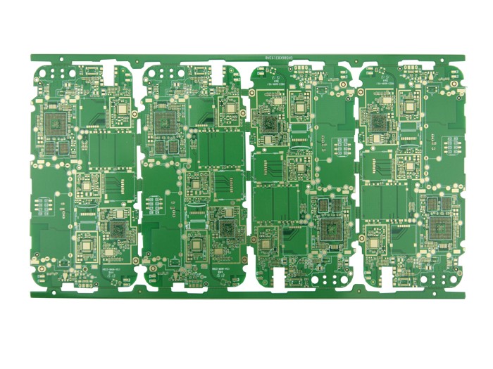
iPCB is a high-tech manufacturing enterprise focusing on the development and production of high-precision PCBs. iPCB is happy to be your business partner. Our business goal is to become the most professional prototyping PCB manufacturer in the world. Mainly focus on microwave high frequency PCB, high frequency mixed pressure, ultra-high multi-layer IC testing, from 1+ to 6+ HDI, Anylayer HDI, IC Substrate, IC test board, rigid flexible PCB, ordinary multi-layer FR4 PCB, etc. Products are widely used in industry 4.0, communications, industrial control, digital, power, computers, automobiles, medical, aerospace, instrumentation, Internet of Things and other fields.