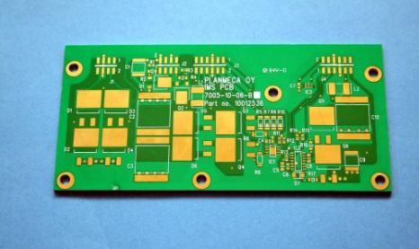
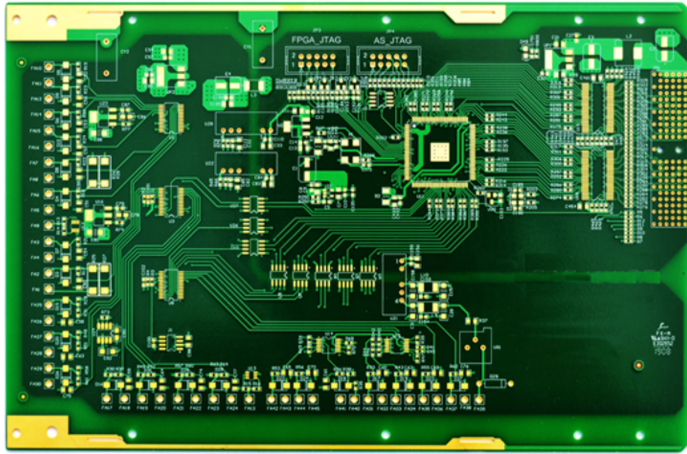
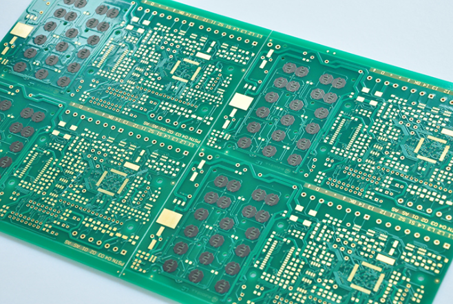
Understand the role of each layer of the PCB board in a penny second
Just above, we have introduced what layers a PCB board has, and briefly introduced the name of each board layer. Today we will take a closer look at the specific functions of each layer of the PCB board. PCB circuit boards are generally divided into six layers, specifically: mechanical layer, forbidden wiring layer, solder resist layer, solder flux layer, silk screen layer and via layer.

Mechanical layer
Protel 99 SE provides 16 mechanical layers, which are generally used to set the external dimensions of the circuit board, data marks, alignment marks, assembly instructions and other mechanical information. This information varies depending on the requirements of the design company or PCB manufacturer. Executing the menu command Design|MechanicalLayer can set more mechanical layers for the circuit board. In addition, the mechanical layer can be added to other layers to output and display together.
Prohibited wiring layer
Used to define the area where components and wiring can be effectively placed on the circuit board. Draw a closed area on this layer as the effective area for routing. Automatic layout and routing is not possible outside this area.
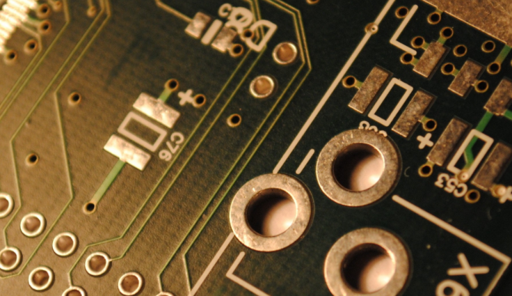
Solder mask
Apply a layer of paint, such as solder resist, to all parts other than the pads to prevent tin on these parts. The solder mask is used to match the pads during the design process and is automatically generated.
Soldering layer
The soldering layer is used for machine patching. It corresponds to the pads of all patch components. The size is the same as the top/bottom layer. It is used to open the stencil to leak tin.
Silk screen
The silk screen layer is mainly used to place printed information, such as component outlines and annotations, various annotation characters, etc. Protel 99 SE provides two silk screen layers, Top Overlay and Bottom Overlay. Generally, all kinds of marked characters are on the top silk screen layer, and the bottom silk screen layer can be closed.
Drilling layer
The drilling layer provides drilling information during the circuit board manufacturing process (such as pads and vias need to be drilled). Protel 99 SE provides two drilling layers, Drillgride (drilling indication map) and Drill drawing (drilling drawing).
The role of each layer of the PCB board
Although the sparrow is small, it has all five internal organs-PCB circuit board can be said to carry out such an old saying. The main development direction of PCB circuit boards is also small and precise. Therefore, for each layer of circuit boards, technicians need to choose carefully and carefully solder them in order to provide more sophisticated PCB circuit boards for major manufacturers and individuals.