PCB layer introduction and definition of each layer
PCB board layers are divided into: signal layer, internal power layer, silk screen layer, mechanical layer and shielding layer. The following editor will introduce the definition of each layer of PCB.
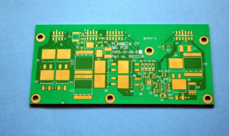
PCB layer introduction
Signal layer
The Signal Layers include the Top Layer, Bottom Layer and Mid-Layer.
The top signal layer is also called the component layer, the main purpose is to place the components, but for the double-layer PCB and multilayer PCB, it can be used to arrange wires or copper.
The bottom signal layer is also called the soldering layer, which is mainly used for wiring and welding, but for double-layer PCB boards and multilayer PCB boards, it is a place where components can be placed.

The middle layer is usually used for arranging signal lines in a multilayer board(not including power lines and ground lines), and can have up to 30 layers.
The top, bottom and middle layers can be connected to each other through vias (Via or Through Hole), blind vias (Blind Via) and buried vias (Buried Via).
Internal power layer
The internal power layer is the inner electric layer. The number of PCB board layers we often say refers to the sum of the signal layer and the inner electric layer. The inner electric layer and the inner electric layer, and the inner electric layer and the signal layer can also be connected to each other through through holes, blind holes, and buried holes, just like signals.
Silk screen
The purpose of the silk screen layer is to place the outlines and annotations of some components, various annotation characters and other printed information, so as to facilitate the soldering and circuit inspection of the later components. The silk screen layer is usually white, and a circuit board can have 2 silk screen layers, divided into the top silk screen layer (Top Overlay) and the bottom silk screen layer (Bottom Overlay).
The top silk screen layer is mainly used to mark the projection outline of the components, the label of the component, the nominal value or model, and various annotation characters.
The bottom silk screen layer has the same function as the top silk screen layer. If the top silk screen layer can contain all the label information, the bottom silk screen layer can be turned off
Mechanical layer
Mechanical Layers (Mechanical Layers) are generally used to place indicative information about board manufacturing and assembly methods, such as PCB dimensions, size markings, data materials, via information, assembly instructions and other information.
Masking layer
Altium Designer provides two mask layers with both top and bottom layers: Solder Mask and Paste Mask.
The assembly solder layer refers to the part that needs to be painted green on the PCB board, because it is a negative output, so the part of the solder mask that is really effective is not the solder mask oil, but the silver-white tin plated.
The solder paste layer is used for machine placement. It corresponds to the pads of all patch components. The size is the same as the Top Layer/Bottom Layer layer. It is used to open the stencil to leak tin.
The paste absorption layer is only used when the machine is patched, and corresponds to the pads of all patch components. It is the same size as the Top Layer/Bottom Layer layer and is used to open the stencil to leak tin.
The above is the relevant knowledge introduced by the PCB board layer, I hope it will be helpful to you!