What are the general PCB board making process?
What are the general PCB manufacturing processes? PCB production is generally divided into: PCB layout- core board production - inner PCB layout transfer - core board punching and inspection - lamination - drilling - copper chemical precipitation on the hole wall - outer PCB layout transfer - computer control and electroplating copper. The specific operation process is as follows:
01 PCB layout (Layout)
After the PCB manufacturer receives the customer’s CAD file, because each CAD software has its own unique file format, the PCB manufacturer generally converts the CAD file sent by the customer into a unified format-Extended Gerber RS-274X or Gerber X2. The engineer then checks whether the PCB layout conforms to the manufacturing process and whether there are defects.
02 Production of core board
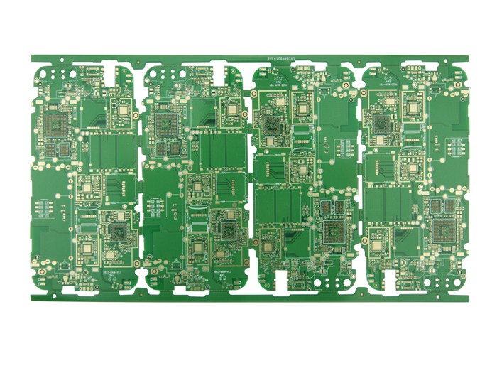
Clean the copper clad laminate to prevent the circuit from being short-circuited or broken due to dust. The figure below is an example of an 8-layer PCB, which is actually made up of 3 copper clad laminates(core boards) plus 2 copper films, and then glued together with prepregs. The production sequence is to start with the middle core board (4 and 5 layers of circuits), continuously stack together, and then fix. The production of 4-layer PCB is similar, except that only one core board and two copper films are used.
03 Inner PCB layout transfer
First, make the two-layer circuit of the middle core board (Core). After the copper clad laminate is cleaned, it will be covered with a photosensitive film on the surface. This film will solidify when exposed to light, forming a protective film on the copper foil of the copper clad laminate. Insert the two-layer PCB layout film and the double-layer copper clad laminate, and finally insert the upper PCB layout film to ensure that the upper and lower PCB layout films are stacked accurately

The photosensitive machine irradiates the photosensitive film on the copper foil with a UV lamp. The photosensitive film is cured under the light-transmitting film, and there is still no cured photosensitive film under the opaque film. The copper foil covered under the cured photosensitive film is the required PCB layout circuit, and then the uncured photosensitive film is cleaned with lye. The required copper foil circuit will be covered by the cured photosensitive film. Then use a strong base, such as NaOH, to etch away the unnecessary copper foil. Tear off the cured photosensitive film to expose the copper foil of the required PCB layout.
04 Core board punching and inspection
After the core board is successfully manufactured, align holes are punched on the core board to facilitate alignment with other materials.
Once the core board is pressed together with other layers of PCB, it cannot be modified, so inspection is very important. The machine automatically compares with the PCB layout drawing to check for errors. In this way, the first two layers of PCB boards have been made.
05 Laminating
A new raw material is needed here called prepreg (Prepreg), which is the adhesive between the core board and the core board (the number of PCB layers>4), as well as the core board and the outer copper foil, and it also acts as an insulation. The lower copper foil and the two layers of prepreg have been fixed in advance through the alignment hole and the lower iron plate, and then the finished core board is also placed in the alignment hole, and finally the two layers of prepreg, a layer of copper foil and A layer of pressure-bearing aluminum plate covers the core plate.
The PCB boards clamped by the iron plates are placed on the support, and then sent to the vacuum heat press for laminating. The high temperature in the vacuum hot press can melt the epoxy resin in the prepreg and fix the core boards and copper foils together under pressure. After the lamination is completed, remove the upper iron plate that presses the PCB. Then remove the pressure-bearing aluminum plate. The aluminum plate also has the responsibility of isolating different PCBs and ensuring the smoothness of the outer copper foil of the PCB. Both sides of the PCB taken out at this time will be covered by a layer of smooth copper foil
06 Drilling
First, drill through the through-hole through the PCB, and then metalize the hole wall to conduct electricity. Put a layer of aluminum plate on the punching machine machine, and then put the PCB on it. In order to improve efficiency, according to the number of PCB layers, 1 to 3 identical PCB boards are stacked together for perforation. Finally, cover the uppermost PCB with a layer of aluminum plate. The upper and lower layers of aluminum plate are used to prevent the copper foil on the PCB from tearing when the drill bit drills in and out.
Next, the operator only needs to select the correct drilling program, and the rest is done automatically by the drilling machine. The drill bit of the drilling machine is driven by air pressure, and the maximum rotation speed can reach 150,000 revolutions per minute. Such a high rotation speed is sufficient to ensure the smoothness of the hole wall. The replacement of the drill bit is also automatically completed by the machine according to the program. The smallest drill bit can reach a diameter of 100 microns, while the diameter of a human hair is 150 microns. Because in the previous lamination process, the melted epoxy resin was squeezed out of the PCB, so it needs to be cut off. The profiling milling machine cuts its periphery according to the correct XY coordinates of the PCB.
07 Chemical precipitation of copper on the hole wall
In the first step, a layer of conductive material is deposited on the hole wall, and a 1 micron copper film is formed on the entire PCB surface by chemical deposition, including the hole wall. The entire process such as chemical treatment and cleaning is controlled by the machine.
08 Outer PCB layout transfer
The transfer of the outer PCB layout adopts the normal method, and the positive film is used as the board. The PCB layout of the outer layer is transferred to the copper foil, and the PCB layout is transferred to the copper foil by using photo-printed film and photosensitive film. The non-circuit area is covered by the cured photosensitive film on the PCB. After cleaning the uncured photosensitive film, electroplating is performed. Where there is a film, it cannot be electroplated, and where there is no film, copper is plated first and then tin is plated. After the film is removed, alkaline etching is performed, and finally the tin is removed. The circuit pattern remains on the board because it is protected by tin.
Put the cleaned PCB on both sides of the copper foil into the laminating machine, and the laminating machine will press the photosensitive mold onto the copper foil. Fix the printed PCB layout film of the upper and lower layers through the positioning holes, and put the PCB board in the middle. Then, the photosensitive film under the light-transmitting film is cured by the irradiation of the UV lamp, which is the circuit that needs to be reserved. After cleaning off the unnecessary and uncured photosensitive film, inspect it. Clamp the PCB with clamps, and electroplate the copper. In order to ensure adequate conductivity of the hole, the copper film plated on the hole wall must have a thickness of 25 microns, so the entire system will be automatically controlled by a computer to ensure its accuracy.
09Computer control and copper electroplating
After the copper film is electroplated, the computer will arrange to electroplate a thin layer of tin. After unloading the tin-plated PCB board, check to ensure that the thickness of the plated copper and tin is correct. Next, a complete automated assembly line completes the etching process. First, clean the cured photosensitive film on the PCB. Then use a strong alkali to clean the unnecessary copper foil covered by it. Then use the tin stripping solution to strip the tin plating on the PCB layout copper foil. After cleaning, the 4-layer PCB layout is completed.