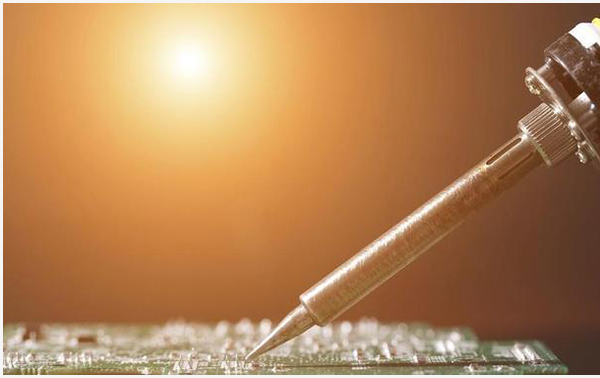
What are the reasons why PCB produces tin beads?
There are four reasons for PCB to produce tin beads. Let's take a look at the four of them:
1. The production of tin beads is related to flux.
Flux will remain under the components or between the PCB board and the carrier (tray for selective soldering). If the flux is not sufficiently preheated and burned out before the PCB board touches the tin wave, tin spattering will occur and tin beads will be formed. Therefore, the preheating parameters recommended by the flux supplier should be strictly followed.

Whether the tin beads adhere to the PCB board depends on the substrate material. If the adhesive force between the tin beads and the PCB board is less than the weight of the tin beads, the tin beads will bounce off the board and fall back into the tin tank. In this case, the solder mask is a very important factor. The rough solder mask will have a smaller contact surface with the tin balls, and the tin balls are not easy to stick to the PCB circuit board. In the lead-free soldering process, the high temperature will make the solder mask more smooth and more likely to cause tin beads to stick to the board.
2. Tin beads produced by outgassing of volatile substances in PCB board and solder mask.
If there are cracks in the metal layer of the through holes of the PCB board, the volatilized gas after heating of these substances will escape from the cracks and form tin beads on the component surface of the PCB board.
3. Tin beads formed when the PCB circuit board leaves the liquid solder.
When the PCB board is separated from the tin wave, the circuit board will pull out the tin pillar, and when the tin pillar breaks and falls back to the tin tank, the splashed solder will fall on the board to form tin beads. Therefore, when designing the tin wave generator and tin tank, attention should be paid to reducing the drop height of tin. The small landing height helps reduce tin dross and tin splashing. The use of nitrogen will aggravate the formation of tin beads. The nitrogen atmosphere can prevent the formation of an oxide layer on the surface of the solder, increasing the probability of the formation of tin beads. At the same time, nitrogen will also affect the surface tension of the solder.
4. The reason for the steel mesh
The stencil hole is to allow the solder paste to leak to the PCB pad. The opening has an inclination angle (such as 45 degrees). Ideally, the shape and thickness of the solder paste remaining on the pad are good when demolding.
Although there are many reasons for PCB to produce tin bead, the more common reason through analysis is caused by steel mesh.