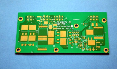
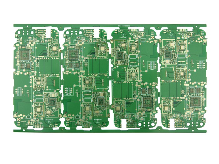
Understand the method and steps of PCB copying in one penny
Simply put, PCB copying is to scan the circuit board to be copied, record the location of the components in detail, and then disassemble the components on the original circuit board to make a BOM list for purchase, and scan the remaining light boards into The picture is processed and restored by the copy board software to a PCB board drawing file. With the PCB file, you can find a suitable PCB manufacturer to make the board, and then solder the purchased components to the finished PCB board, and finally the circuit board Perform testing and debugging.
Let's take a look at the PCB copy board method and steps:
The first step: get the PCB board that needs to be copied, first take a few photos of the component position with the camera, especially the direction of the diode, the direction of the tertiary tube, and the direction of the IC gap. Then record the models, parameters and positions of all vitality parts on the paper in detail.

Step 2: Remove all the components on the circuit board, copy the board files, and remove the tin in the PAD hole. Clean the PCB with alcohol and put it in the scanner. When the scanner scans, you need to raise the scanned pixels slightly to get a clearer image.
Slightly polish the top and bottom layers with water gauze paper until the copper film is shiny, put them in the scanner, start PHOTOSHOP, and scan the two layers separately in color.
Note: The PCB must be placed horizontally and vertically in the scanner, otherwise the scanned image cannot be used.
The third step: adjust the contrast and brightness of the canvas to make the part with copper film and the part without copper film have a strong contrast, then turn the second image into black and white, and check whether the lines are clear. If it is not clear, repeat this step. If it is clear, save the picture as black and white BMP format files TOP.BMP and BOT.BMP. If you find any problems with the graphics, you can also use PHOTOSHOP to repair and correct them.
Step 4: Convert the two BMP format files to PROTEL format files respectively, and transfer two layers in PROTEL. If the positions of the PAD and VIA on the two layers basically coincide, it indicates that the previous steps are well done. If there is a deviation, repeat the third step.
Step 5: Convert the BMP of the TOP layer to TOP.PCB. Pay attention to the conversion to the SILK layer, which is the yellow layer, and then trace the line on the TOP layer, and place the device according to the drawing in the second step. Delete the SILK layer after drawing. Keep repeating until all the layers are drawn.
Step 6: Import TOP.PCB and BOT.PCB in PROTEL and combine them into one picture.
The seventh step is to use a laser printer to print the TOP LAYER and BOTTOM LAYER on the transparent film at a ratio of 1:1. Put the film on the PCB and compare whether there is any error. If it is correct, the board copy is basically completed. Finally, perform a performance test on the copied PCB board. If the performance is the same as the original PCB, it means that the copy board is completely completed.
If you are copying a multi-layer board, you need to carefully polish it to the inner layer, and repeat the copying steps from the third to the fifth step. Of course, the naming of the graphics is also different. It depends on the number of layers. Generally, double-sided copying is more than The laminate is much simpler, and it is prone to misalignment when copying the multi-layer board, so the multi-layer board should be especially careful and careful (the internal vias and non-vias are prone to problems).