What are the effects of copper clad PCB board?
The so-called copper pour is to use the unused space on the PCB as a reference surface and then fill it with solid copper. These copper areas are also called copper filling. So, what is the role of copper clad PCB board?
The significance of copper coating is to reduce the impedance of the ground wire and improve the anti-interference ability; reduce the voltage drop and improve the efficiency of the power supply; when connected to the ground wire, it can also reduce the loop area.
There are generally two ways to pour copper: large-area copper pour and grid copper.
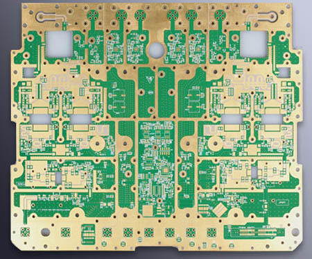
Copper Clad Circuit Board
Large-area copper coating has the dual functions of increasing current and shielding. However, if a large area of copper is covered, if wave soldering is used, the board may be uplifted or even blistered. Therefore, for large-area copper coating, several grooves are usually opened to relieve the blistering of the copper foil.

The pure copper-clad grid is mainly used for shielding, and the effect of increasing the current is reduced. From the perspective of heat dissipation, the grid reduces the heating surface of the copper and plays a role in electromagnetic shielding to a certain extent. Especially for touch and other circuits.
It should be pointed out that the grid is made up of traces in staggered directions. For the circuit, the width of the trace has a corresponding "electrical length" for the operating frequency of the circuit board. When the operating frequency is not very high, perhaps the effect of the grid lines is not obvious. Once the electrical length matches the operating frequency, you will find that the circuit does not work properly at all, and signals that interfere with the operation of the system are emitted everywhere.
Which copper pour method to use depends on the working conditions of the designed circuit board. Multi-purpose grids with high anti-interference requirements for high-frequency circuits, and circuits with large currents in low-frequency circuits are commonly used and complete copper.
iPCB is a high-tech manufacturing enterprise focusing on the development and production of high-precision PCBs. iPCB is happy to be your business partner. Our business goal is to become the most professional prototyping PCB manufacturer in the world. Mainly focus on microwave high frequency PCB, high frequency mixed pressure, ultra-high multi-layer IC testing, from 1+ to 6+ HDI, Anylayer HDI, IC Substrate, IC test board, rigid flexible PCB, ordinary multi-layer FR4 PCB, etc. Products are widely used in industry 4.0, communications, industrial control, digital, power, computers, automobiles, medical, aerospace, instrumentation, Internet of Things and other fields.