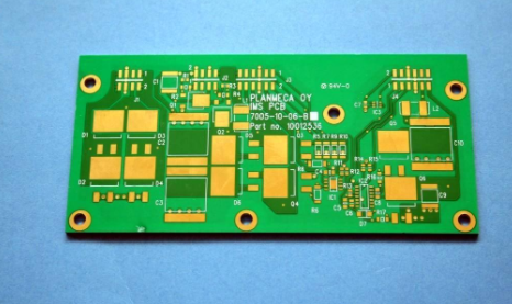
Knowledge point: PCB board wiring process
Before we design the PCB board, we must understand the wiring process of the PCB board. Let me explain in detail for you below:
PCB board wiring process
1. Drawing the correct schematic diagram and network table schematic diagram is the prerequisite for designing the PCB board, and the network table is the bridge connecting the schematic diagram and the PCB board diagram.
2, determine the component package, complete the conversion from the schematic to the PCB. Protel99SE provides a wealth of standard component libraries. Before importing the netlist file, the PCB component package library must be loaded to ensure that all used libraries have been loaded.
3. Set environmental parameters. Set environmental parameters according to your own habits, such as grid size, cursor capture size, conversion of metric and imperial units, etc. In addition, the layers of the PCB board must be set.

4. Plan the circuit board. It is mainly to set various physical parameters of the circuit board, including whether the circuit board adopts a double-layer board or a multilayer board, the shape and size of the circuit board, and the installation method of the circuit board.
5. Import the network table. The net list contains the packaging form of each component and the connection relationship between the components. Importing the net list will get the basis for the subsequent design of the PCB.
6. Layout of components. First lay out the components related to the mechanical size and lock these components, then lay out the larger and more space-consuming components and the core components of the circuit, and finally lay out the peripheral small components.
7. Develop detailed wiring rules. Wiring rules include wiring spacing, various line widths, via size, wiring topology, etc., which need to be set according to the actual situation of the design. In addition, place a filler layer in areas where traces are not desired.
8, PCB wiring. This step includes three steps: manual wiring, automatic wiring and manual adjustment.
9. The processing of the terminal of the circuit board. In the design, the power supply, grounding, signal input and output terminals must be connected to the outside world, and the lead-out method depends on the process requirements. The common lead-out method is to use the pad to lead out and to use the connector to lead out.
10. Copper coating and tear-filling. In order to enhance the anti-interference ability of the circuit board, it is necessary to deposit copper on the ground wire network of each wiring layer. In addition, all vias and pads need to be filled with teardrops.
11. Carry out design rule check. In order to ensure that the circuit board diagram complies with the design rules and that all networks have been correctly connected, a design rule check must be done after the wiring is completed.
12. Adjust the information on the remaining layers. After passing the design rule check, drag and drop all the characters of the silk screen layer to the appropriate position, and finally put the printing plate name, design version number, company name, file first processing date and other information.
13. Save and export printed board files. After the design is completed, the printed board files must be sorted, archived and printed drawings. In addition, you can export the component list, generate a spreadsheet file as a component list, and so on.
The above is the PCB board wiring process explained in detail by the editor, I hope it will be helpful to you.