Professional PCB manufacturers explain the circuit board processing flow for you in detail
In electronic equipment, the printed circuit board is a key part, known as the "mother of electronic products." Circuit boards can be divided into single-sided, double-sided, and multilayer circuit boards:
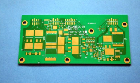
Circuit board processing flow
[Single Panel] On the most basic PCB, the parts are concentrated on one side, and the wires are concentrated on the other side.
[Double-sided board] This kind of circuit board has wiring on both sides, but to use the wires on both sides, there must be a proper circuit connection between the two sides. The "bridge" between such circuits is called a via.
[Multilayer board] In order to increase the area that can be wired, more single or double-sided wiring boards are used for multilayer boards. Usually the number of layers is even.
The following is the circuit board processing process explained by professional PCB manufacturers in detail for you
1. The copper foil substrate is cut into a size suitable for processing according to the requirements of the design drawings.
2. Before pressing the film, use brushing, micro-etching and other methods to properly roughen the copper foil on the board surface, and then attach the dry film photoresist to it at a certain temperature and pressure.
3. The substrate is sent to an ultraviolet exposure machine for exposure, and the photoresist is irradiated by ultraviolet rays to produce a polymerization reaction, and the circuit image on the negative film is transferred to the dry film photoresist of the board.
4. Tear off the protective film on the membrane surface, first use the sodium carbonate aqueous solution to develop and remove the unlit area on the membrane surface, and then use the hydrogen peroxide mixed solution to corrode and remove the exposed copper foil to form a circuit.
5. Finally, the dry film photoresist is washed off with a lightly oxidized sodium water solution.

1. Before pressing, the inner layer board is blackened (oxidized) to passivate the copper surface to increase insulation; and the copper surface of the inner layer circuit is roughened to produce good adhesion performance.
2. When pressing, firstly rive the multi-layer (more than six layers) inner circuit boards with a riveting machine in pairs, and then send them into the vacuum pressing machine to harden and bond the film with appropriate temperature and pressure.
3. Use the X-ray automatic positioning target drilling machine to drill the target hole as a reference hole for the alignment of the inner and outer layers; and properly fine-cut the edge of the board to facilitate subsequent processing.
[Drilling] The circuit board is drilled with a CNC drilling machine to drill the through holes of the interlayer circuit and the fixing holes of the welded parts; when drilling, use the pin to penetrate the previously drilled target hole to fix the circuit board to the drill Hole on the machine tool.
[Plated through holes] After the interlayer vias are formed, a metal copper layer needs to be laid on the board to complete the interlayer circuit conduction. First clean the hair on the hole and the powder in the hole, and then soak and attach tin to the cleaned hole wall.
[One-time copper] Immerse the circuit board in a chemical copper solution. With the catalytic effect of palladium metal, the copper ions in the solution are reduced and deposited on the wall of the hole to form a through-hole circuit; and then electroplated in a copper sulfate bath, Thicken the copper layer in the via hole to a thickness sufficient for subsequent processing.
[Outer circuit secondary copper] The circuit image transfer is the same as the inner circuit, but the circuit etching is divided into two production methods, positive film and negative film. The production method of negative film is the same as the production of inner layer circuit. After development, the copper is directly etched and the film is removed. The positive film production method is to add secondary copper and tin-lead plating after development. After removing the film, the exposed copper foil is corroded and removed with a mixed solution of alkaline ammonia water and copper chloride to form a circuit. Finally, the tin-lead layer is stripped with tin-lead stripping solution.
[Solder Resistant Ink Text Printing] Early green paint was produced by direct thermal drying (or ultraviolet irradiation) after screen printing to harden the paint film. Nowadays, photosensitive green paint is mostly used for production. The text, trademark or part number required by the customer is printed on the board surface by screen printing, and then the text lacquer ink is hardened by heat drying (or ultraviolet irradiation).
[Contact processing] The solder mask green paint covers most of the copper surface of the circuit, and only the terminal contacts for part welding, electrical testing and circuit board insertion are exposed. This terminal needs to be added with a suitable protective layer to avoid affecting the stability of the circuit.
[Forming and cutting] The circuit board is cut into the external size required by the customer with a CNC molding machine (or die punch). After cutting, the golden finger parts are processed with bevel angle. Finally, clean the powder and ionic contaminants on the circuit board.
[Check board packaging] PE film packaging, heat shrinkable film packaging or vacuum packaging are commonly used.
The above is the circuit board processing process detailed by professional PCB manufacturers. ipcb is a high-precision and high-quality PCB manufacturer, such as: isola 370hr PCB, high-frequency PCB, high-speed PCB, ic substrate, ic test board, impedance PCB, HDI PCB, Rigid-Flex PCB, buried blind via PCB, advanced PCB, microwave PCB, telfon PCB and other ipcb are good at PCB manufacturing.