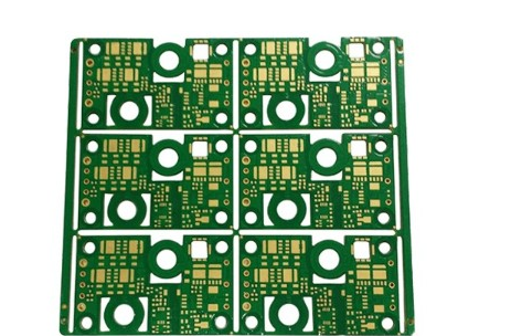
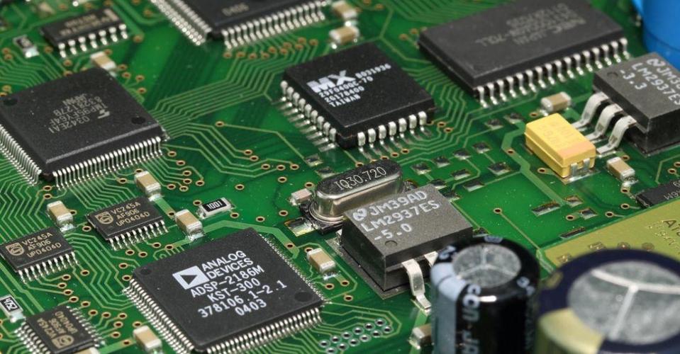
The iPhone 7 is coming, and everyone is talking about how gorgeous the curved screen of the iPhone 7 is, how cool the 3D touch technology is, and it can be waterproof and wirelessly charged. The growth rate of its black technology is comparable to the arms race during the Cold War. Duo Ren, as engineering students, we want to defend our dignity in the topic, perhaps we need to analyze its essence through these cool appearance functions, for example, its entire "skeleton"-circuit board, scientific name PCB .
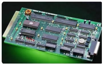
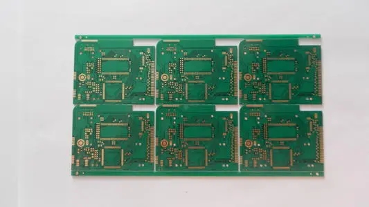
PCB, that is, Printed Circuit Board, is not only a support for electronic components, but also a carrier for electrical connection of electronic components. Before the advent of PCB, the connection between electronic components was completed by direct connection of wires; but now, the wire connection method is only used in laboratory tests, and PCB has occupied an absolute control position in the electronics industry.

Talk about history, the past and present of PCB
The development history of PCB can be traced back to the early 20th century. In 1936, the Austrian Paul Eisler (Paul Eisler) applied PCB in the radio, putting PCB into practical use for the first time; in 1943, the United States widely used the technology in military radios; in 1948, the United States officially recognized that the invention can be used For commercial use. As a result, PCB began to be widely used since the mid-1950s, and then entered a period of rapid development.
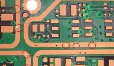
As PCBs become more and more complex, when designers use development tools to design PCBs, it is easy to confuse the definition and purpose of each layer. When our hardware developers draw the PCB by themselves, it is easy to cause unnecessary misunderstandings in production because they are not familiar with the purpose of each layer of the PCB. In order to avoid this situation, here we take Altium Designer Summer 09 as an example to classify and introduce the PCB layers.
Differences between PCB layers
Signal Layers
Altium Designer can provide up to 32 signal layers, including Top Layer, Bottom Layer and Mid-Layer. The layers can be connected to each other through vias, blind vias and buried vias.
1. The top signal layer (Top Layer)
Also called the component layer, it is mainly used to place components. For double-layer boards and multilayer boards, it can be used to arrange wires or copper.
2. Bottom Layer
Also called soldering layer, it is mainly used for wiring and soldering. For double-layer boards and multilayer boards, it can be used to place components.
3. Mid-Layers
There can be up to 30 layers, which are used to arrange signal lines in a multilayer board. Power lines and ground lines are not included here.
Internal Planes
Usually referred to as the inner electric layer for short, it only appears in multi-layer boards. The number of PCB board layers generally refers to the sum of the signal layer and the inner electric layer. Same as the signal layer, the inner electric layer and the inner electric layer, and the inner electric layer and the signal layer can be connected to each other through through holes, blind holes and buried holes.