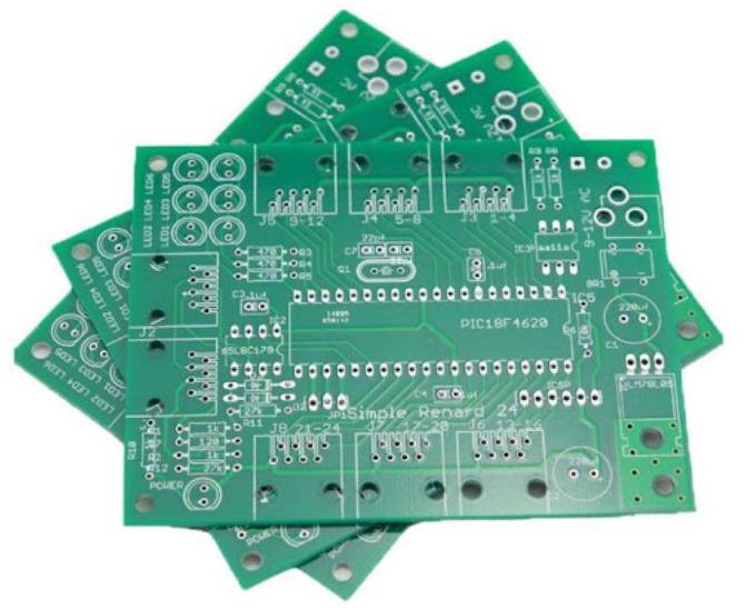
Get to know the via process in PCB proofing
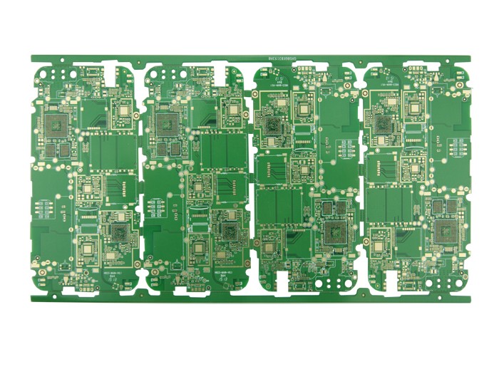
Vias are one of the important components of multilayer PCBs, and the cost of drilling usually accounts for 30% to 40% of the cost of PCB proofing. From the point of view of function, vias are divided into two categories: one is used for electrical connections between layers; the other is used for fixing or positioning devices. From the process of PCB proofing, vias are divided into three categories, namely blind holes, buried holes and through holes.
Through holes refer to holes that pass through the entire circuit board, which can be used for internal interconnection or as a component's installation positioning hole. Because the through hole is easier to implement in the process and the cost is lower, it is used in most printed circuit boards instead of the other two types of through holes.

Next, let's focus on blind vias and buried vias.
Blind holes are located on the top and bottom surfaces of the printed circuit board and have a certain depth. They are used for the connection of the surface circuit and the inner circuit. The depth of the hole usually does not exceed a certain ratio (aperture). Buried hole refers to the connection hole located in the inner layer of the printed circuit board, which does not extend to the surface of the circuit board. The above two types of holes are located in the inner layer of the circuit board, and are completed by a through-hole forming process before lamination, and several inner layers may be overlapped during the formation of the via. The application of blind vias and buried vias greatly reduces the size and quality of HDI (High Density Interconnect) PCBs, reduces the number of layers, improves electromagnetic compatibility, increases the characteristics of electronic products, reduces costs, and also makes the design work easier and faster .
In PCB proofing, blind holes and buried holes are special processes, which are difficult and have a high error rate, so they are expensive, and some PCB manufacturers seldom do it. ipcb is a high-precision, high-quality PCB manufacturer, such as: isola 370hr PCB, high-frequency PCB, high-speed PCB, ic substrate, ic test board, impedance PCB, HDI PCB, Rigid-Flex PCB, buried blind PCB, advanced PCB, microwave PCB, telfon PCB and other ipcb are good at PCB manufacturing.