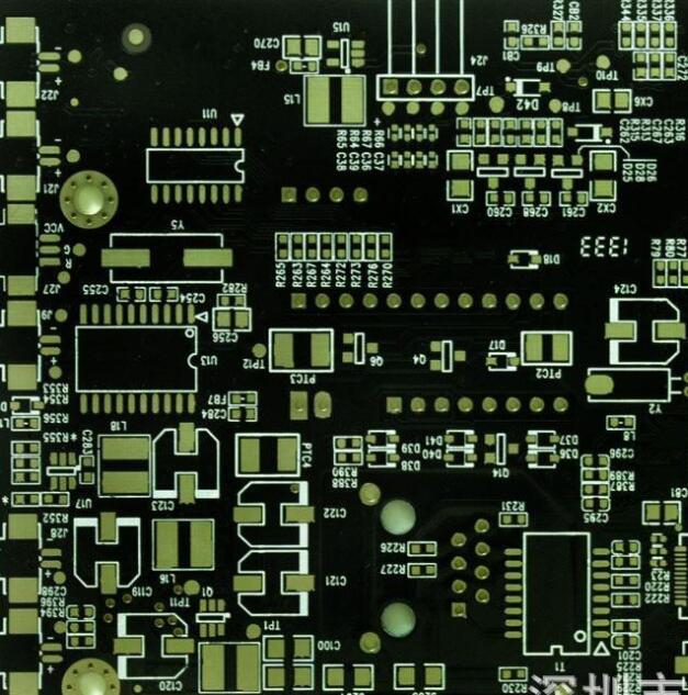
The solution to the problem of negative film deformation in the PCB board process
1. The cause and solution of film deformation
reason
(1) Temperature and humidity control failure.
(2) The exposure machine temperature rises too high.
Solution
(1) Normally, the temperature is controlled at 22±2 degree Celsius, and the humidity is at 55%±5%RH.
(2) Adopt a cold light source or aerator with the cooling device and constantly replace the backup file.

2. Technological method of film deformation correction
1. Under the condition of mastering the operating technology of the digital programming instrument, first install the negative film and compare it with the drilling test board, measure its length and width two deformations, and lengthen or shorten the hole position according to the deformation amount on the digital programming instrument, Use the drilled test board after lengthening or shortening the hole position to adapt to the deformed negative film, eliminating the troublesome work of cutting the negative film, and ensuring the integrity and accuracy of the graphics. Call this method "change hole position method".
2. In view of the physical phenomenon that the negative film changes with the environmental temperature and humidity, take out the negative film in the sealed bag before copying the negative film, and hang it for 4-8 hours in the working environment so that the negative film will be deformed before copying. It will make the negative film after copying very small, and this method is called the "hanging method".
3. For graphics with simple lines, large line widths, spacing, and irregular deformations, you can cut the deformed part of the negative film to contrast the hole positions of the drill test board and re-splice before copying. This method is called the "splicing method".
4. Use the holes on the test board to enlarge the pads to remove the heavy deformation of the circuit piece to ensure the minimum ring width technical requirements. This method is called the "pad overlap method".
5. After scaling up the graphics on the deformed negative film, re-map and make a plate, call this method "map method".
6. Use a camera to enlarge or reduce the deformed figure. This method is called the "photographic method".
3. Points for attention in related methods:
1, splicing method
Applicable: Negative film with less dense lines and inconsistent deformation of each layer of the film, especially suitable for the deformation of solder mask film and multi-layer board power layer film.
Not applicable: Negative film with high wire density, line width, and spacing less than 0.2mm;
Note: When splicing, the wires should be damaged as little as possible, and the pads should not be damaged. When revising the version after splicing and copying, attention should be paid to the correctness of the connection relationship.
2, change the hole position method:
Applicable: The deformation of each layer of the film is the same. This method is also applicable to film with dense lines;
Not applicable: The film is deformed unevenly, and the local deformation is particularly serious.
Note: After using the programming instrument to lengthen or shorten the hole position, the out-of-tolerance hole position should be reset.
3. Hanging method:
Applicable; Films that have not been deformed and prevented from deforming after copying;
Not applicable: Deformed film.
Note: Hang the film in a ventilated and dark environment (safety is also possible) to avoid contamination. Ensure that the temperature and humidity of the hanging place is the same as that of the working place.
4. Pad overlap method:
Applicable: The graphic lines are not too dense, and the line width and spacing are greater than 0.30mm;
Not applicable: especially users have strict requirements on the appearance of printed circuit boards.
Note: After the overlapping copy, the pad is elliptical. After overlapping and copying, the halo and distortion of the edge of the line and disk.
5. Photographic method:
Applicable: When the ratio of deformation in the length and width directions of the negative film is the same, and it is inconvenient to re-drill the test board, only the silver salt film can be used.
Not applicable: The length and width direction of the negative film are not deformed.
Note: The focus should be accurate when taking pictures to prevent distortion of the lines. Negative film loss is more, usually, after many times of debugging are required to obtain a satisfactory circuit pattern.
ipcb is a high-precision, high-quality PCB manufacturer, such as isola 370hr PCB, high-frequency PCB, high-speed PCB, ic substrate, ic test board, impedance PCB, HDI PCB, Rigid-Flex PCB, buried blind PCB, advanced PCB, microwave PCB, Teflon PCB, and other ipcb are good at PCB manufacturing.