Application of image surveying and mapping instrument to PCB board detection
PCB factory: The two-dimensional image measuring instrument (also known as the image surveying and mapping instrument) is based on the CCD digital image, and is produced by relying on the powerful software capabilities of computer screen measurement technology and spatial geometric calculations. After the computer is installed with special control and graphic measurement software, it becomes a measurement brain with the soul of the software, which is the main body of the entire device.
working principle
The two-dimensional image measuring instrument uses its own hardware (CCD, eyepiece, objective lens data line, video capture card) to transmit the captured images to the computer data capture card through the data line, and then the software will image on the computer monitor. The operator uses the mouse to make quick measurements on the computer. The above process is basically completed in tens of thousands of seconds, so it can be regarded as a real-time detection device, or a narrower point can be called a dynamic measurement device. If the configuration meets the requirements, the device will never produce image lag. Depending on the size of the workpiece, different strokes can be selected for the worktable. The brightness of the light source is adjustable, and the most suitable light source brightness can be selected under various light conditions.
The application of two-dimensional image measuring instrument to PCB detection
In the application of image measuring instrument, PCB inspection technology is not introduced much. Let me introduce the application in this area
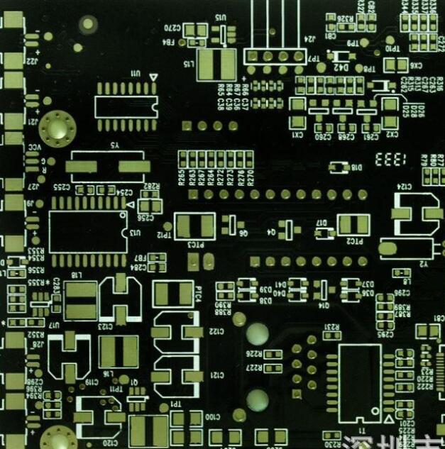
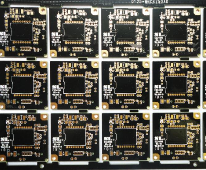
First of all, in the PCB industry, the two-dimensional image measuring instrument is mainly used to measure the appearance of high-density PCBs. Nowadays, customers are gradually moving towards the requirements for the appearance of PCB boards based on the strict requirements of the original electrical performance. Its shape tolerance also tends to be harsh, so image measuring instrument tools just make up for this gap, and even more so many PCB manufacturers prefer more precise three-dimensional measuring instruments.

2. In addition, on the level of possible horizontal expansion, the image measuring instrument can also be used for the measurement of PCB film, which is suitable for a high-tech inspection of production tools in the plate making process. Through the data provided by the project, the distance between any points of the PCB film is measured by the second element, and the data list is obtained for analysis, so that the expansion and contraction coefficient of the PCB film can be obtained scientifically, which can assist the production more scientifically.
Because of the so-called PCB inspection, we mostly use the desired instrument to detect the length, width and height of the PCB, so generally we can use the two-dimensional image measuring instrument to detect, of course, for the detection of the PCB height, we can use the two-dimensional image Probes are added on the basis of the instrument to achieve the purpose of simple three-dimensional inspection, and this is more than enough for PCB high inspection.
In terms of PCB inspection technology and inspection equipment, we can clearly see from the above introduction that the use of a two-dimensional image measuring instrument to complete the detection of PCB related parameters is completely achievable by a two-dimensional image instrument and can achieve high Complete PCB-related inspection tasks with quality.
iPCB is a high-tech manufacturing enterprise focusing on the development and production of high-precision PCBs. iPCB is happy to be your business partner. Our business goal is to become the most professional prototyping PCB manufacturer in the world. Mainly focus on microwave high frequency PCB, high frequency mixed pressure, ultra-high multi-layer IC testing, from 1+ to 6+ HDI, Anylayer HDI, IC Substrate, IC test board, rigid flexible PCB, ordinary multi-layer FR4 PCB, etc. Products are widely used in industry 4.0, communications, industrial control, digital, power, computers, automobiles, medical, aerospace, instrumentation, Internet of Things and other fields.