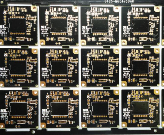
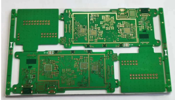
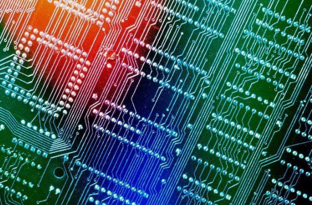
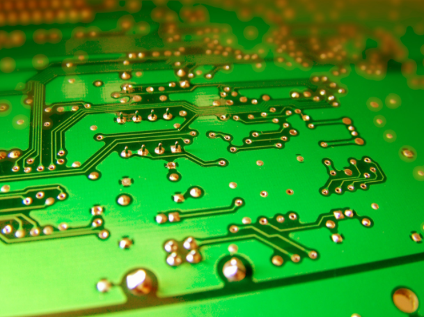
Introduce two surface treatment methods of copper foil
PCB factory: We all know that the surface treatment of copper foil is generally divided into the following two types:
Traditional treatment
After the ED copper foil is torn off from the Drum, the following processing steps will be continued:
Bonding Stage-Plating copper on the matte side with high current in a very short time, its appearance is like a tumor, which is called "nodulization" and "Nodulization" The purpose is to increase the surface area, and its thickness is about 2000~4000A
Thermal barrier treatments-After the tumor is formed, a layer of brass (Brass, patented by Gould, called JTC treatment), or zinc (Zinc, patented by Yates Corporation, called TW treatment) is plated on it. Also nickel plating is used as a heat-resistant layer. Dicy in the resin will attack the copper surface at high temperature to generate amines and moisture. Once moisture is generated, the adhesion will decrease. The function of this layer is to prevent the above reaction from happening, and its thickness is about 500~1000A
Stabilization-After heat-resistant treatment, the final "chromation" (Chromation) is carried out. The smooth and rough surfaces are simultaneously used as anti-fouling and anti-rust effects, also called "passivation" (passivation) or "anti-oxidation" "Treatment" (antioxidant) However, this method of treatment has rarely been used at present.
New approach

Double treatment refers to the roughening treatment of both smooth and rough surfaces. Strictly speaking, the application of this method has a history of 20 years, but today there are more and more users to reduce the cost of multilayer boards. The above-mentioned traditional processing method is also performed on the smooth surface. When applied to the inner substrate in this way, the copper surface treatment and the black/browning step before lamination can be omitted. A processing method developed by a Polyclad copper foil substrate company in the United States, called DST copper foil, is similar in approach. In this method, the smooth surface is roughened, and the surface is pressed on the film. The copper surface of the substrate is rough, so it is also helpful for post-production.
Siliconization (Low profile) is now used in most PCB factories.
In short, the Tooth Profile roughness (peak and trough) of the traditional copper foil rough surface treatment is not conducive to the manufacture of fine lines (affects the just etch time and causes over-etch), so we must try to reduce the height of the ridge. The above-mentioned Polyclad DST copper foil is treated with a smooth surface to improve this problem. In addition, a kind of "Organic Silane Treatment" (Organic Silane Treatment) can also have this effect after adding traditional treatment methods. It also creates a chemical bond, which is helpful for adhesion.
iPCB is a high-tech manufacturing enterprise focusing on the development and production of high-precision PCBs. iPCB is happy to be your business partner. Our business goal is to become the most professional prototyping PCB manufacturer in the world. Mainly focus on microwave high frequency PCB, high frequency mixed pressure, ultra-high multi-layer IC testing, from 1+ to 6+ HDI, Anylayer HDI, IC Substrate, IC test board, rigid flexible PCB, ordinary multi-layer FR4 PCB, etc. Products are widely used in industry 4.0, communications, industrial control, digital, power, computers, automobiles, medical, aerospace, instrumentation, Internet of Things and other fields.