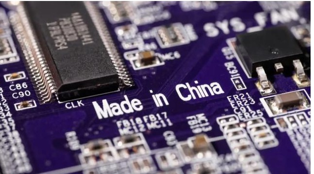
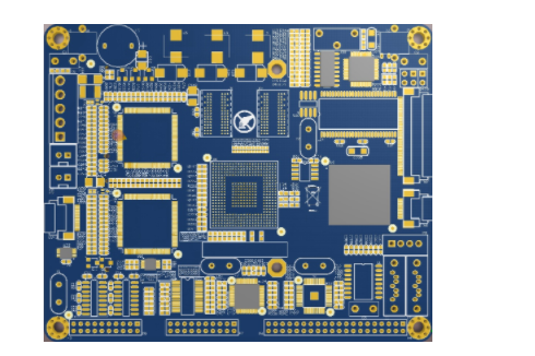
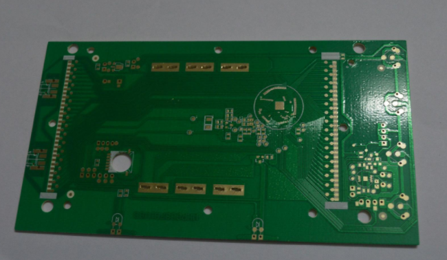
High-precision HDI circuit board manufacturer
High-precision HDI circuit boardmanufacturers. With the advancing of the information time, Laizi's electrical products have also made corresponding progress. Many people are demanding more and more electrical products, which are high, light, and thin. Many people are interested in electronics. Product appearance requirements, multi-functionality are half of the external requirements for people. The high integration of the body core guide and the rapid increase in the number of I/Os, plus the requirements for the degree, density, precision and reliability of the multi-layer printing, and the multi-printing layer of the new build method manufacturing layer is satisfactory The above new requirements for printed circuit boards have been implemented, but they are not only highly precise, high-density features, but also highly feasible. It can be seen from the development history of printing to circuit board that the basic development and printing of the infrastructure is the prerequisite for the high level of board manufacturing. This article mainly studies the manufacturing process, main techniques and existing problems of the blind hole multilayer printed circuit board. 3 Problems existing in the printing technology of the blind porous layer system. Regarding the problem of the appropriate weight between the layers of the blind via structure layer and the multi-layer printed board, this is the probability of the successful manufacturing of the blind multi-hole printed board by Wengao. It borrowed the pre-pinning system of the multi-pass layer printed board., Make sure to set the layer's single-piece and every-pattern production in the front system of the positioning system.

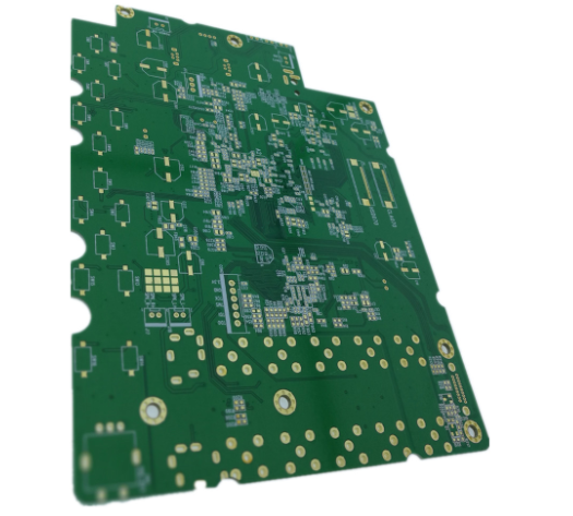
In order to allow faster progress in electronic communication technology. High-quality high-speed transmission, many of today's communication facilities use high-frequency printed multilayer PCB circuit boards. The materials of multilayer high-frequency circuit boards have good electrical functions and better chemical stability. The main ones are as follows Four major points:
1. It has the special characteristics of low loss of signal transmission, short delay time of transmission, and low distortion of signal transmission.
2. Possess excellent dielectric properties (mainly: low relative permittivity Dk, low dielectric loss factor Df). Moreover, this special dielectric property (Dk, Df) can maintain its stability even under the background changes of frequency, humidity, and temperature.
3. High-precision control with special impedance (Zo).
4. Possess particularly good heat resistance (Tg), processability and suitability.
Based on the above special properties, high-frequency boards are widely used in communication facilities such as wireless receiving antennas, base station antennas, power amplifiers, components (splitters, combiners, and showers), radar systems, and navigation systems.
Multi-layer high-frequency circuit boards are preset, based on cost savings, increased buckling strength, electromagnetic interference suppression, and other factors, often exposed in the form of mixed plates, called high-frequency mixed plates. The selection of high-frequency mixed materials and the implementation of stacking combinations are numerous and exhaustive. After development, Mingyi Electronics produced a multi-layer high-frequency circuit board in an experiment, and considered it appropriate and used the combination of high-frequency materials RO4350B/RO4450B and FR4 materials. The final results of the trial production of HDI circuit board manufacturers show that the prefabrication of multi-layer high-frequency hybrid circuit boards is based on one or more factors of cost saving, increased buckling strength, and electromagnetic interference suppression. In the process, high-frequency prepregs with low natural resin fluidity and FR-4 substrates with a smoother appearance of the medium. Under such circumstances, there is a greater risk of controlling the adhesion of the product during the pressing process.
Experiments show that through the selection of FR-4 A material, the presetting of the spherical flow glue baffle block at the edge of the plate, the use of pressure-releasing materials, and the use of key technologies such as the control system of the pressure parameters, the successful realization of the mixed pressure material The adhesion of the circuit board is satisfactory, and the reliability of the circuit board is not abnormal after the test. The material of high-frequency circuit boards for electronic communication products is indeed a good choice.
The square method of image non-linear proofreading is discussed. After the CCD image sensor collects the circuit board image, the imaging optical system originally has a special property that the digital image has non-linear distortion, which affects the accuracy of the survey. The distorted image is corrected from two aspects: position correction and gray correction. First establish the distortion proofreading board type, select the typical distortion image and propose to obtain the ideal coordinates of the characteristic landmark points and the coordinates of the actual distortion points, and use the optimal approximate solution idea under the minimum square error criterion to solve the distortion coefficient; then substitute the distortion coefficient into the distortion plate The position correction of the entire distorted image was successfully achieved in the model; because the final result of the position correction is not necessarily the number of flat heads, it was finally deemed appropriate and used bilinear interpolation to perform gray-scale correction. Experiments show that the correction of distortion has achieved satisfactory results.
Principle of Immersion Gold
Immersion of gold on the nickel surface is a kind of displacement reaction. When nickel is immersed in a solution containing Au(CN)2-, it is eroded by the solution and throws out 2 electrons, and is immediately caught by Au(CN)2- and quickly precipitates Au on the nickel: 2Au(CN) 2-+Ni-2Au+Ni2++4CN
The thickness of the immersion gold layer is generally between 0.03 and 0.1μm, but at most it should not exceed 0.15μm. It has a satisfactory effect of taking care of the things that nickel covers the face and has good contact and conduction performance. Many electronic devices (such as mobile phones, electronic dictionaries) that require button contact are deemed appropriate and use chemical immersion gold to try their best to take care of the nickel surface. In addition, it should be pointed out that the welding performance of the electroless nickel/gold plating layer is shown by the nickel layer, and the gold is only provided to take care of the solderability of the nickel as much as possible. The thickness of gold as a solderable plating layer should not be too high, otherwise it will cause brittleness and weak solder joints, but if the gold layer is too thin, the protection performance will deteriorate.
PCB preset requires metallized via interconnection introduction
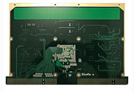
The active feed network combines the requirements of high performance, multi-function, high reliability, low damage, complete amplitude and phase, small-scale and light-weight requirements, and provides PCB presets and production belts for multi-layer microwave printed circuit boards. It is very difficult. For this reason, the different functions of the PCB are preset on different layers, such as the combination of mixed signal lines such as microstrip lines, strip lines, and low-frequency choke lines in the same multi-layer structure, through multiple types of metal The production of chemical holes successfully realized DC interconnection. High precision HDI circuit board
Vertical interconnection is the main form of successful realization of interconnection between circuits of different layers in microwave multilayer circuits. The vertical interconnection is mainly successfully realized by metallized blind vias and buried vias. In view of the preset requirements of the PCB, the same-layer circuits in the inner layer will be connected to the upper and lower circuits at the same time. Because of this, the research on depth-controlled drilling technology has become certain.
Shenzhen Audemars Piguet Circuit Co., Ltd. (iPCB.cn) resolutely maintains the basis of market competition with high-quality products, quick delivery, complete services, satisfactory credit, and flexible marketing. Its business has expanded to Europe, Many countries and regions in the New World, Asia and Australia. The purpose of the future is to establish the world's largest production platform in the field of prototypes, small and medium-sized batches, a senior technical team in the manufacturing industry, and experience in the growth of comprehensive technical solutions in the field of electronic hardware presets, and a set of multi-variety rapid processing services. Experience, provide customers with personalized one-stop service.