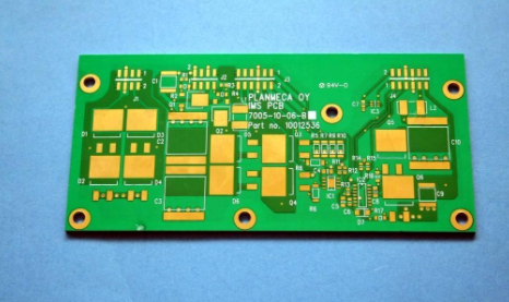
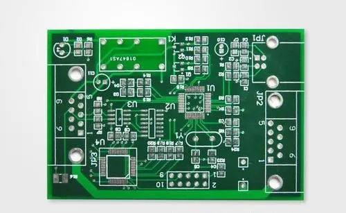
hdi multilayer board
High-density interconnect printed circuit boards use the latest technology to manufacture printed circuit boards in the same or smaller area to increase the use of functions.
This has promoted major advances in mobile and computer products, resulting in revolutionary new products. This includes touch screen computers, 4G communications and military applications such as avionics and smart military equipment.
High-density interconnect (HDI) printed circuit boards have high-density characteristics, including laser microvias, fine wires, and high-performance thin materials. This increased density supports more features per unit area.
High-tech high-density interconnection (HDI) printed circuit boards contain multilayer stacked copper-filled microvias (high-end HDI printed circuit boards), which can be used to make more complex interconnections.
These very complex structures provide the necessary wiring solutions for the large pin number chips used in today's mobile devices and other high-tech products.

These micro-holes are formed by laser drilling, and their diameters are usually 0.006μm, (150μm), 0.005μm, (125μm) or 0.004μm (100μm), which are related to the corresponding pad diameter of 0.012μm.
(300μm), 0.010≤ quotation; (250μm) or 0.008μm; (200μm) alignment to obtain more wiring density.
The micro-holes can be designed directly on the pad or deviate from each other, can be interlaced or superimposed, can be filled with non-conductive resin, and the surface can be electroplated with copper cover or directly electroplated to fill the holes.
The microvia design is valuable when wiring fine pitch BGAs (such as 0.8mm pitch and below chips).
In addition, when wiring 0.5mm pitch components, a staggered microvia structure can be used, but when wiring micro BGAs (such as 0.4mm, 0.3mm or 0.25mm pitch components), stacked microvias (SMV?) are required.
It is realized by inverted pyramid wiring technology. Lianshuo has many years of experience in the production of high-density interconnect (HDI) products, which are second-generation microvias or stacked microvias (SMV?).
This technology provides a pioneer of true copper layer microvias supporting micro-BGA wiring solutions.
The table below shows Lianshuo's complete microporous technology. Lianshuo has developed a third-generation microvia or NextGen-SMV?, Can greatly shorten the manufacturing time of stacked microplates (5-7 days).
NextGenSMV? This technology realizes the rapid production of printed circuit boards with complex conductive hole structures, requiring only one layer, while reducing thermal shock (heat loss of materials) and the entire production cycle time.
NextGE-SMV? It can not only eliminate the production cycle of internal copper plating, but also increase impedance tolerance, reduce overall thickness and improve electrical characteristics.
In addition, NextGen-SMV? Any layer of interconnection can be realized by metal bonding between the conductive plasma and copper on the inner wire, which provides flexibility for designers. ipcb is a high-precision, high-quality PCB manufacturer, such as: isola 370hr PCB, high-frequency PCB, high-speed PCB, ic substrate, ic test board, impedance PCB, HDI PCB, Rigid-Flex PCB, buried blind PCB, advanced PCB, microwave PCB, telfon PCB and other ipcb are good at PCB manufacturing.