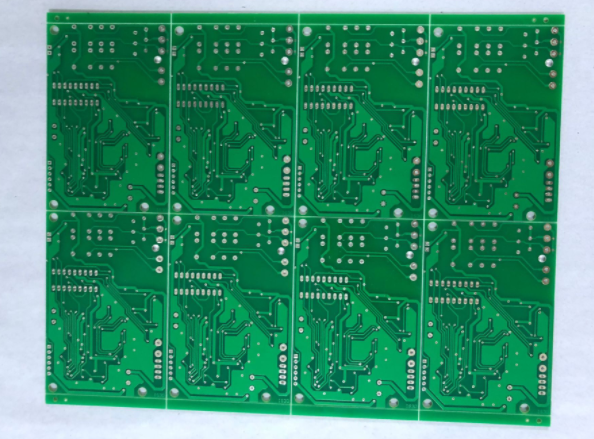
Five minutes to watch the production process of foreign multilayer circuit boards
Single and double panels: according to the size optimized by the plan, open the material - sanding treatment - drilling - pressing the circuit board - electroplating blind hole - making outer circuit - circuit oil printing - oven drying - smoothing treatment - exposure machine exposure (film Positioning)-Developing on the developing machine in the dark room-etching-printing green oil-baking-printing white letters and characters-gong edge-open and short circuit function test-enter FQC-final inspection, visual inspection-vacuum packaging after cleaning.
Multi-layer circuit boards: Active optical inspection and visual inspection are required before pressing to enter the press for typesetting and pressing (in a vacuum environment) - arrange in a fixed large and small mold - 2 hours cold pressing, 2 hours hot pressing - segmentation Demolition - Cutting according to the size optimized in the plan - Grinding treatment - Drilling - Pressing circuit board- Plating blind holes - Making outer circuit - Line oil printing - Oven drying - Smoothing treatment - Exposure machine exposure (Film positioning )-Developing on the developing machine in the dark room-etching-printing green oil-baking-printing white characters and characters-gong edge-open and short circuit function test-enter FQC-final inspection, visual inspection-vacuum packaging after cleaning.

Now the editor briefly introduces the functions of each layer of the circuit board as follows:
⑴Signal layer: mainly used to place components or wiring. Protel DXP usually includes 30 middle layers, namely Mid Layer1~Mid Layer30. The middle layer is used to place signal lines, and the top and bottom layers are used to place components or deposit copper.
⑵Protection layer: It is mainly used to ensure that the parts of the circuit board that do not need to be tinned are not tinned, and then to ensure the reliability of the circuit board operation. Among them, Top Paste and Bottom Paste are the top solder mask and the bottom solder mask respectively; Top Solder and Bottom Solder are the solder paste protective layer and the bottom solder paste protective layer, respectively.
⑶ Silk screen layer: mainly used to print the serial number, production number, company name, etc. of the components on the circuit board.
⑷Internal layer: mainly used as signal wiring layer, Protel DXP includes 16 internal layers.
⑸ Other layers: mainly includes 4 types of layers.
Drill Guide (drilling azimuth layer): It is mainly used for the position of drilling holes on the printed circuit board.
Keep-Out Layer (prohibited wiring layer): mainly used to make the electrical frame of the circuit board.
Drill Drawing (drilling drawing layer): mainly used to set the drill shape.
Multi-Layer (multi-layer): Mainly used to set multi-layer.