A wiring engineer talks about PCB design experience
PCB wiring technology-a wiring engineer talks about PCB design experience
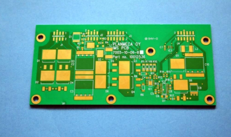
The general PCB design process is as follows: preliminary preparation -> PCB structure design -> PCB layout -> wiring -> wiring optimization and silk screen printing -> network and DRC inspection and structure inspection -> plate making. "
First: Preliminary preparation. This includes preparing component libraries and schematics. "If you want to do well, you must first sharpen your tools." To make a good board, in addition to designing the principles, you must also draw well. Before proceeding with PCB design, we must first prepare the component library of the schematic SCH and the component library of the PCB. The component library can use Peotel's own library, but it is generally difficult to find a suitable one. It is best to make your own component library based on the standard size data of the selected device. In principle, do the PCB component library first, and then do the SCH component library. The PCB component library requirements are high, which directly affects the installation of the board; the SCH component library requirements are relatively loose, as long as you pay attention to the definition of the pin attributes and the corresponding relationship with the PCB components. PS: Pay attention to the hidden pins in the standard library. After that is the design of the schematic diagram, and when it is done, it is ready to start the PCB design.

Second: PCB structure design. In this step, draw the PCB surface in the PCB design environment according to the determined circuit board size and various mechanical positioning, and place the required connectors, buttons/switches, screw holes, assembly holes, etc. according to the positioning requirements. And fully consider and determine the wiring area and non-wiring area (such as how much area around the screw hole belongs to the non-wiring area).
Third: PCB layout. To put it plainly, the layout is to put devices on the board. At this time, if all the preparations mentioned above are done, you can generate the netlist (Design->Create Netlist) on the schematic, and then import the netlist (Design->Load Nets) on the PCB diagram. You can see the whole stack of devices crashing, and there are flying wires between the pins to indicate the connection. Then you can lay out the device. The general layout is carried out according to the following principles:
1. . According to the reasonable division of electrical performance, it is generally divided into: digital circuit area (that is, afraid of interference and interference), analog circuit area (fear of interference), power drive area (interference source)
2. . Circuits that complete the same function should be placed as close as possible, and the components should be adjusted to ensure the most concise connection; at the same time, adjust the relative position between the functional blocks to make the connection between the functional blocks the most concise;
3. . For high-quality components, the installation location and installation strength should be considered; heating components should be placed separately from temperature-sensitive components, and heat convection measures should be considered when necessary;
4. . The I/O drive device is as close as possible to the edge of the printed board and to the lead-out connector;
5. . The clock generator (such as crystal oscillator or clock oscillator) should be as close as possible to the device that uses the clock;
6. . Between the power input pin of each integrated circuit and the ground, a decoupling capacitor (generally a monolithic capacitor with good high-frequency performance is used); when the board space is dense, one can also be added around several integrated circuits Tantalum capacitors.
7. . A discharge diode should be added to the relay coil
8. . The layout requirements should be balanced, dense and orderly, not top-heavy or heavy
--Special attention is needed. When placing components, the actual size of the components (occupied area and height) and the relative position between the components must be considered to ensure the electrical performance of the circuit board and the feasibility of production and installation At the same time as convenience, the placement of the components should be appropriately modified under the premise of ensuring that the above principles can be reflected to make them neat and beautiful. For example, the same components should be placed neatly and in the same direction.
This step is related to the overall image of the board and the difficulty of wiring in the next step, so a little effort must be taken into consideration. When laying out, you can make preliminary wiring and fully consider the places that are not sure about it.