How to distinguish between PCB board and integrated circuit
The circuit board at this stage is specifically composed of the following combinations:
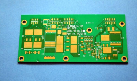
Route and pattern (Pattern): Route is used as a tool to communicate between the originals. In the structural design, another large copper surface is designed as a grounding protection and power layer. The new line and the cad drawing are made at the same time.
Dielectric layer (Dielectric): used to maintain the insulation between the route and the layers, also known as the metal substrate.
Hole (Through hole / via): Via hole can make
The routes on the two levels are connected to each other. The oversized vias are used as part software. In addition, non-vias (nPTH) are generally used as surface layer placement for precise positioning and are used for fixing screws during assembly.
Solder resistant /Solder Mask: Not all copper surfaces must eat tin parts, so the non-tin area will be printed with a layer of substance that blocks the copper surface from eating tin (usually epoxy resin). Prevent short circuits between non-tin-eating routes. According to different processes, it can be divided into green oil, red oil and blue oil.
Silk screen (Legend/Marking/Silk screen): This is a non-essential composition. The primary function is to mark the name and position frame of each part on the PCB, which is convenient for maintenance and identification after assembly.

Surface Finish: Because the copper surface is easy to oxidize in the air in the general environment, it can not be tinned (poor solderability), so it will be maintained on the copper surface that needs to be tinned. The protection methods include HASL, ENIG, Immersion Silver, Immersion TIn, and Organic Solder Preservative (OSP). The advantages and disadvantages of each method are collectively referred to as the electroplating process.
PCB board features
Can be high-density. For decades, the high-density of printed boards has been developed with time-lapse integrated circuit chip integration and continuous advancement in mounting technology.
High reliability. According to various inspections, tests and aging tests, the long-term (use period, generally 20 years) and reliable operation of the PCB can be guaranteed.
Designability. Regarding the various properties of PCB boards (electrical, physical, chemical, mechanical, etc.), the printed board design can be realized according to the design standard vertebralization, standardization, etc., in a short time and high efficiency.
Manufacturability. Using intelligent management, it can carry out standardized management, scale (quantity) production, and automation technology to ensure product quality consistency.
Testability. A relatively complete test method, test standard, various test equipment and instruments have been established to detect and appraise the eligibility and warranty period of PCB products.
Can be assembled. PCB products are not only convenient for standardized assembly of various components, but also for mechanical automation and large-scale mass production. At the same time, PCBs and various components can be assembled to form larger parts, systems, and even complete machines.
Maintainability. Because PCB products and various component assembly parts are in accordance with standardized design and professional production, these components are also standardized. These, once the system software fails, it can be disassembled and replaced more quickly, conveniently, and flexibly, and the operating system can be quickly restored to work. Of course, there are more examples. Such as miniaturization and weight reduction of the system, and high-speed signal transmission.
Features of integrated circuit chip
Integrated circuit chips have the advantages of small size, light weight, fewer lead wires and solder joints, durability, high reliability indicators, and good performance. At the same time, they are low-cost, which is conducive to mass production. It is not only widely used in industrial and civil communication equipment such as radio cassette recorders, flat-screen TVs, and electronic computers, but also in national defense, communications, and remote control. Using integrated circuit chips to assemble electronic products, the assembly density can be increased several to several thousand times than that of transistors, and the stable working hours of machinery and equipment can also be greatly improved.