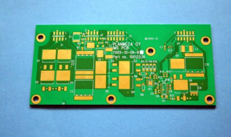
About the causes of poor PCB soldering
1. The solderability of the circuit board hole affects the welding quality
The solderability of the circuit board hole is not good, and the defect of false soldering will occur, which will affect the parameters of the components in the circuit, resulting in unstable conduction of the multi-layer board component and the inner line, causing the function of the entire circuit to fail. The so-called solderability is the property that the metal surface is wetted by the molten solder, that is, the solder addresses the metal surface to form a relatively uniform continuous smooth adhesion film. The main factors that affect the solderability of printed circuit boards are:
(1) The composition of the solder and the nature of the solder. Solder is an important part of the soldering chemical treatment process. It is composed of chemical materials containing flux. Commonly used low-melting eutectic metals are Sn-Pb or Sn-Pb-Ag. The impurity content must be controlled by a certain percentage., To prevent the oxides generated by impurities from being dissolved by the flux. The function of the flux is to help the solder to wet the surface of the circuit being soldered by transferring heat and removing rust. White rosin and isopropanol solvents are generally used.
(2) The welding temperature and the cleanliness of the surface of the metal plate also affect the weldability. If the temperature is too high, the loosening speed of the solder will be accelerated. At this time, it will have a high activity, which will cause the circuit board and the solder surface to be oxidized sensitively, and soldering defects will occur. The contamination of the circuit board surface will also affect the solderability and then the defects will occur. These shortcomings Including tin beads, tin balls, open circuits, poor gloss, etc.
2. Welding defects caused by warpage
The circuit board and the component parts warp during the soldering process, and the shortcomings such as virtual soldering and short-circuit due to stress and deformation occur. Warpage is often caused by the unbalanced temperature of the upper and lower parts of the circuit board. For large PCBs, warping will also occur due to the weight of the board itself. The general PBGA equipment is about 0.5mm apart from the printed circuit board. Assuming that the equipment on the circuit board is large, the solder joints will be under stress for a long time after the circuit board is cooled down. It is enough to cause false soldering if the equipment is lifted by 0.1mm. open circuit.

3, the planning of the circuit board affects the welding quality
In the layout, when the circuit board standard is too large, although the soldering is easier to control, the printed lines are long, the impedance increases, the anti-noise ability decreases, and the cost increases; if it is too small, the heat dissipation decreases, the soldering is difficult to control, and adjacent lines are easy to appear. Mutual interference, such as electromagnetic interference of circuit boards.
Therefore, it is necessary to optimize PCB board planning:
(1) Shorten the wiring between high-frequency components and reduce EMI interference.
(2) Components with heavy weight (such as exceeding 20g) should be fixed with brackets and then welded.
(3) Heat dissipation issues should be considered for heating elements, to prevent defects and rework with large ΔT on the surface of the elements, and heat sensitive elements should be far away from the heating source.
(4) The components are placed as parallel as possible, so that they are not only beautiful and easy to solder, but also suitable for mass production. It is best to plan the circuit board as a 4:3 rectangle. Do not change the width of the wire to prevent disconnection of the wiring. When the circuit board is heated for a long time, the copper foil will simply swell and fall. Therefore, the use of large-area copper foil should be avoided.