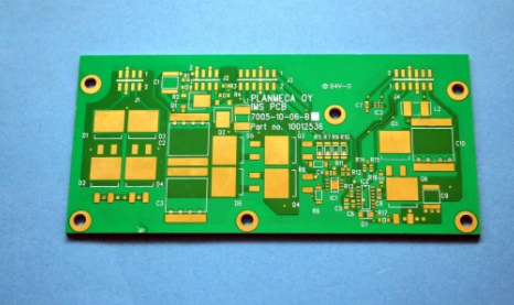
The basic design process of the circuit board can be divided into the following three steps:

(1) The design of the circuit schematic diagram: The design of the circuit schematic diagram mainly uses the schematic diagram editor of Protel DXP to draw the schematic diagram.
(2) Generate printed circuit board reports: After the printed circuit board design is completed, various reports need to be generated, such as generating pin reports, circuit board information reports, network status reports, etc., and finally print out the printed circuit diagram.
(3) The design of the printed circuit board: the design of the printed circuit board is what we usually call the PCB design, which is the final form of the circuit schematic.
The composition of the PCB circuit board(car dashboard)
1. The reception of the circuit board and the drawing surface: The circuit is used as a tool for the conduction between the originals. In the design, a large copper surface will be additionally designed as a grounding and power layer.
2. Dielectric layer: Used to maintain the insulation between the circuit and each layer, commonly known as the substrate.
3. Hole (Through hole / via): The through hole can make the lines of more than two levels connect to each other, the larger through hole is used as a part plug-in, and there are non-through holes (nPTH) usually used as the surface Placement and positioning, for fixing screws during assembly.
4. Solder resistant /Solder Mask: Not all copper surfaces need to be tinned parts, so the non-tin area will be printed with a layer of material that isolates the copper surface from eating tin (usually epoxy resin), To avoid short circuits between non-tinned circuits. According to different processes, it is divided into green oil, red oil and blue oil
Design considerations for PCB circuit boards
One, antenna part design
1. The wiring from the Bluetooth IC to the antenna should be smooth or straight;
2. There should be no components, wiring and copper laying around the effective part of the antenna and its lower layer (namely the back);
2. Wiring principle
1. High-speed signal traces should be as short as possible, and key signal traces should be as short as possible;
2. Do not make too many vias in one trace, no more than two vias;
3. The corners of the routing should be as large as possible to be greater than 90 degrees, avoid corners below 90 degrees, and use 90 degrees as little as possible;
4. In double-panel wiring, the wires on both sides should be perpendicular, oblique, or bent to avoid parallel to each other to reduce parasitic coupling;