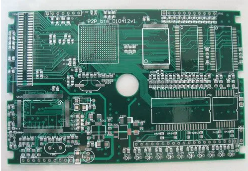
PCB design is based on the circuit schematic diagram to realize the functions required by the circuit designer. PCB design is a very technical work, and it requires many years of experience accumulation. The following circuit board manufacturers have summarized several common problems in PCB circuit design for your reference.

1. Overlap of pads
1. The overlap of the pads (except the surface mount pads) means the overlap of the holes. During the drilling process, the drill bit will be broken due to multiple drilling in one place, resulting in damage to the holes.
2. Two holes in the multilayer board overlap. For example, one hole is an isolation disk and the other hole is a connection pad (flower pad), so that the film will appear as an isolation disk after drawing the film, resulting in scrap.
Second, the abuse of the graphics layer
1. Some useless connections were made on some graphics layers. Originally, it was a four-layer board but designed with more than five layers of wiring, which caused misunderstandings.
2. Save trouble during design. Take the Protel software as an example to draw the lines on each layer with the Board layer, and use the Board layer to mark the lines. In this way, when performing light drawing data, because the Board layer is not selected, it is omitted. The connection is broken, or it may be short-circuited due to the selection of the marking line of the Board layer, so the integrity and clarity of the graphics layer is maintained during design.
3. Violation of conventional design, such as component surface design in Bottom layer and welding surface design in Top, causing inconvenience.
Third, the random placement of characters
1. The SMD soldering pad of the character cover pad brings inconvenience to the continuity test of the printed board and the soldering of the components.
2. The character design is too small, resulting in difficulties in screen printing, and too large will cause the characters to overlap each other and be difficult to distinguish.
Fourth, the setting of the single-sided pad aperture
1. Single-sided pads are generally not drilled. If the drilling needs to be marked, the hole diameter should be designed to be zero. If the numerical value is designed, then when the drilling data is generated, the coordinates of the hole appear at this position, and there is a problem.
2. Single-sided pads should be specially marked if they are drilled.
Five, use filler blocks to draw pads
Drawing pads with filler blocks can pass the DRC inspection when designing the circuit, but it is not good for processing. Therefore, similar pads cannot directly generate solder mask data. When the solder resist is applied, the filler block area will be covered by the solder resist, resulting in It is difficult to solder the device.