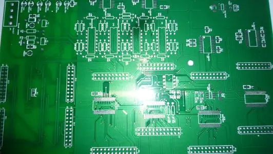
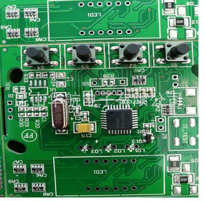
In PCB production, process is an extremely important link, the general process includes OSP, gold plating, tin spraying and so on. Tin spraying as a common process in PCB board production, everyone is familiar with the tin spraying process, and divided into "lead" and "lead-free" two, what is the connection between the two? What difference does it make? I'm going to do it today.
One. Development history
"Lead-free" is developed and evolved on the basis of "lead-free". From the 1990s, the United States, Europe and Japan and other countries enacted legislation on the application of lead in industry, and carried out research on lead-free welding materials and the development of related technologies.

Two, the performance difference
1. Weldability
The melting point of lead-free process is 218 degrees, while the melting point of lead-sprayed tin is 183 degrees. The solderability of lead-free tin welding is higher than that of lead-free tin welding. Lead process is relatively poor fastness, welding is prone to virtual welding. But because lead is present at relatively low temperatures, there is less thermal damage to electronics and the PCB surface is brighter.
2. Cost differences
In the lead-free process, the tin strip used for wave soldering and the tin wire used for manual welding lead to a cost increase of about 3 times; Solder paste used in reflow welding cost increased by about 2 times.
3. Security
As a toxic substance, lead is harmful to human health and environment. Even with lead process has many characteristics, such as prices are low, surface more bright, but under pressure from policy of environmental protection in recent years, has a lead of living space more and more small, reason mainly comes from the PCB with lead process wastewater discharge, and there are lead scrap of PCB products, whether in the form of burying or burning treatment, lead will back into the environment through the media, Thus, lead pollution is serious, which does great harm to the environment and human existence.
With the increasing awareness of environmental protection in China, the Chinese government has also issued relevant laws and regulations on this matter. Since January 1, 2018, the "environmental protection Law" has been implemented, and environmental protection tax has been levied on enterprises, demonstrating the determination of the country to "adjust the structure and promote the transformation". In addition, foreign countries have also issued relevant laws. After the implementation of the EU environmental protection directive, failure to pass the EU means that it cannot enter the European market, thus losing the European market share.
The promulgate of relevant policies and regulations at home and abroad has made many DOMESTIC PCB factories overwhelmed and closed down. The implementation of lead-free is a great challenge for PCB factory, which faces the double test of enterprise quality and technical strength. The good operation of lead-free process is not only the replacement of lead-free production equipment, but also involves the quality of employees, quality management and other aspects, and directly increases the production cost.
On the road from leaded PCB to lead-free PCB, jiepai has strengthened innovation in energy saving and emission reduction, comprehensively applied "big data" and "cloud computing", improved resource utilization rate, realized automatic management and monitoring of production line, and must protect the environment while achieving development.
This is also inseparable from the support of the government. The PCB Industrial Park in Guangde, Anhui province, where the Jet-assembly plant is located, has given full consideration to pollution prevention and centralized control and treatment of pollutants such as sewage and solid waste generated in the production process. After several years of development, Guangde PCB industry has formed a unique "Guangde model". Currently, there are PCB sewage treatment plant, PCB solid waste center, PCB water plant and other supporting projects, which sublimate environmental protection from "important work" to "lifeline".
Only by realizing ecological advantages can PCB enterprises improve their competitiveness, and only by continuous innovation can PCB industry meet the hard target of environmental protection more efficiently and quickly, and finally reduce the operating costs of enterprises. Only when the heavy burden of environmental protection is removed, can PCB industry move forward lightly. Therefore, it is the general trend for PCB enterprises to abandon the "lead" process.