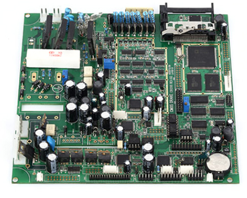
Process characteristics of PCBA communication line card
There are two main types of communication boards-Back Plane and Line Card. The latter is also called a single board.
The backplane is used as the PCB for power supply and signal interconnection between the line cards in the subrack or cabinet. The main features are the thickness, the large size, and the number of layers. Generally, there are no complicated mounting components, and the main components are crimp connectors, and the assembly process is relatively simple.
The line card is the main component of the communication product, and its craftsmanship is embodied in three aspects: high density, high heat dissipation, and high speed. Generally, the size of the line card is relatively large, and there are many types of component packaging used, and it is the most complex type of product among all electronic products.

Structural characteristics of communication line card:
The line card is usually installed in a standard cabinet subrack, instead of using screws to install on the chassis or chassis structure like other electronic products. Therefore, its structure has typical characteristics, with a connector on one side and a panel on the other side. Because the line card is installed on a guide rail, it sometimes needs to be plugged and unplugged during installation and maintenance. Therefore, the line card must meet certain strength requirements and flatness requirements. The communication line card has the following characteristics:
(1) Large size;
(2) There are many types and quantities of component packaging;
(3) The component process requirements vary greatly;
(4) High assembly density;
(5) High power consumption, mostly with radiators;
(6) Long life and high reliability are required.
In addition, in terms of production, it also has a notable feature, that is, "multiple varieties, small batches." These characteristics complicate the communication PCBA assembly process. A certain process has the following characteristics:
(1) The process path is long.
Some components on the communication line card need to use surface assembly process, some need to adopt wave soldering process, and some need to adopt selective wave soldering process or manual soldering process. It is rare to use only one process method to complete the assembly, often multiple The process method is used in combination, so that the process path is relatively long.
(2) The packaging difference is relatively large, and the demand for the amount of solder paste is different.
There are not only components with poor coplanarity and thick solder paste printing on communication line cards, but also components with relatively small pin spacing and thin solder paste printing. Comparing the requirements of these components with different process characteristics becomes the largest process design. Difficulty-the distribution of the amount of solder paste must be considered when the component layout, whether to use the method of expanding the window with steel mesh or the method of using step steel mesh, must be determined in advance and given the minimum implementation space required (the surrounding forbidden area)
(3) There are many assembly operations and many assembly stress sources.
In addition to the welding of electronic components, communication line card assembly also involves operations such as board separation, crimping, screw installation, radiator installation, and stiffener installation. These operations are still manual in many manufacturers, and the operation process often causes PCB damage. Bending, and PCB bending is a common factor that causes chip capacitors to crack and BGA solder joints to break. How to reduce the stress during PCBA assembly is one of the tasks of process design.
ipcb is a high-precision, high-quality PCB manufacturer, such as: isola 370hr PCB, high-frequency PCB, high-speed PCB, ic substrate, ic test board, impedance PCB, HDI PCB, Rigid-Flex PCB, buried blind PCB, advanced PCB, microwave PCB, telfon PCB and other ipcb are good at PCB manufacturing.