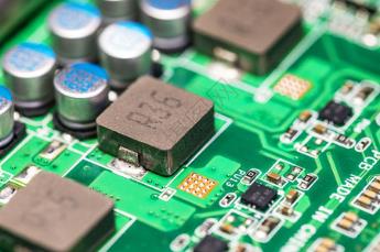
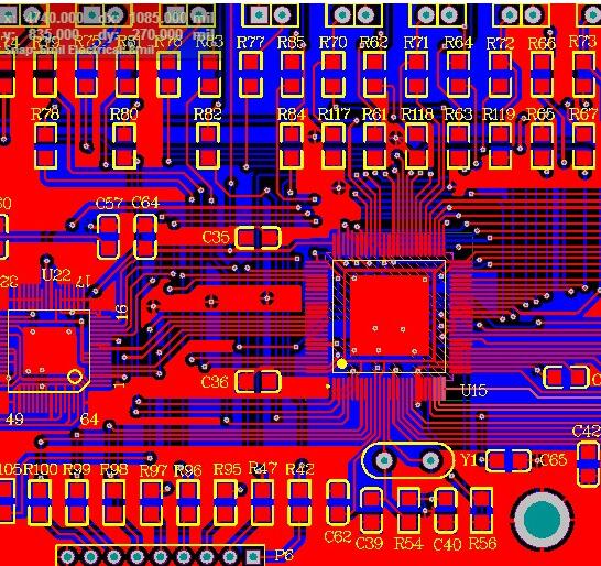
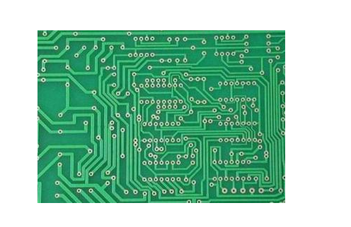
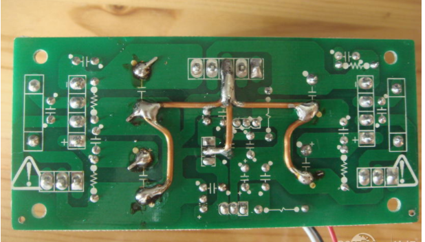
For the PCB copy board design of the motherboard, the routing of various types of signals is a part that has to be paid attention to. Since there are many types of signals designed on the motherboard, and various signal traces have different specifications and requirements, to ensure that the motherboard design is accurate and feasible, it is necessary to have an in-depth understanding of the traces of various signals. Here, we give you a detailed introduction to the wiring specifications and requirements of common signal types in the motherboard design.

1, CPU wiring:
The wiring of the CPU is generally 5/10. The spacing of the control lines should be slightly larger, about 20 mils.
<1>Data lines (0-63) 64 pieces;
<2>Address line (3-31) REQ(0-4) etc.
<3>Control line (generally distributed between the data line and the address line)
When the data lines are routed, every 16 lines are grouped together and run on the same layer.
(0-15) (16-31) (32-47) (48-63) and each group distributes 2-3 control lines,
When the Address lines are routed, every 16 lines are grouped together and run on the same layer. The difference is that the Address lines are not from (3-31) before (0-2). Generally divided into 2 groups,
<1>(3-16) Add 5 REQ lines, 18;
<2>(17-31) 16 pieces;
When the CPU signal is routed, it should be separated from other signals with a 20-30mil GND line, such as DDR signals, to facilitate the use of the inner GND under the VIA and play the role of grounding.
2, DDR signal:
In addition to the Control line, the DDR line is generally 5/10 Control line to maintain a line spacing of 20mil. Like the CPU, it is mainly divided into the following three categories:
<1>Data line (0-63) 64 lines
<2>Address line (0-13) There are also some address signal lines with other names,
<3>Control line (generally distributed between the data and address lines)
When the Data line is routed, every 8 lines are a group, plus 2 DQM and DQS control lines to go together and go on the same layer. The main grouping methods are:
MD (0-7) add DQM0 DQS0
MD (8-15) plus DQM 1 DQS 1
MD (16-23) plus DQM 2 DQS 2
MD (24-31) plus DQM3 DQS 3
MD (32-39) plus DQM 4 DQS 4
MD (40-47) plus DQM 5 DQS 5
MD (48-55) plus DQM 6 DQS 6
MD (56-63) plus DQM 7 DQS 7
Address lines are all together as much as possible;
In addition, there are 3 pairs of CLK lines in the DDR part. If it is a dual-channel DDR, there are 6 pairs of CLK lines. The CLK should be paired and kept at least 20 mils apart from other signals.
DDR, like the CPU, should also be separated from other signals with a 20-30mil GND signal, mainly the CPU and AGP signals
3, CLK signal:
The CLK signal is an important signal in the motherboard, generally as large as the following:
<1>200 trillion
<2>100 trillion
<3>66 trillion
<4>48 trillion
<5>16 trillion
The above is the introduction of various signal routing requirements and techniques for PCB copy board design. Ipcb also provides PCB manufacturers and PCB manufacturing technology.