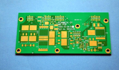
If excessive solder paste is applied to the pad during the PCB assembly process, or the solder paste is insufficiently added, or even no solder paste is placed at all, then after the subsequent reflow soldering, once the solder joints are formed, It will cause defects in the electronic connection between the components and the circuit board. In fact, most of the defects can be found with the help of the application of solder paste to find the relevant quality marks.

At present, many PCB manufacturers have adopted some built-in circuit tests to detect the quality of solder joints, which helps to eliminate the defects caused by the printing process, but these methods cannot monitor the printing process operation itself. The circuit board with the wrong printing may accept the additional process steps, and each process step will increase the production cost to varying degrees, so that such a defective circuit board will eventually reach the placement stage of production. Post-manufacturers need to discard this defective circuit board, or need to accept costly and wasteful repair work. At this moment, there may not be a very clear answer to explain the root cause of the defect.
The built-in vision system can achieve three main goals:
1. The defects can be found directly after the printing operation is implemented, and the operator can deal with the related problems in time before the main manufacturing cost is added to the circuit board. This step generally includes when the circuit board is removed from the printing device, after it is cleaned in the cleaning agent, and when it is returned to the production line after being repaired.
2. Because related defects are discovered at this stage, it can prevent defective circuit boards from being delivered to the back end of the production line, thus preventing the phenomenon of rework or discarding in some cases.
3. It can give the operator feedback in time whether the printing process in operation is good, and thus can effectively prevent the occurrence of defects.
A key function of the advanced online vision system is to be able to perform inspections on highly reflective PCB circuit boards and pad surfaces, as well as inspections under uneven light conditions or under conditions that cause differences in the dry solder paste structure. The inspection of PCB is mainly to detect the printing area, printing offset and bridging phenomenon. The inspection of the printing area refers to the area of solder paste on each pad. Excessive solder paste may cause bridging phenomenon, but too small The solder paste will also cause the phenomenon of weak solder joints. The detection of printing offset is for whether the amount of solder paste on the pad is different from the specified position, and the detection of bridging phenomenon is for whether the solder paste applied between two adjacent pads exceeds the specified value. Quantity, these excess solder paste may cause electrical short circuits.
The detection of printing templates is mainly for the detection of blocking and trailing phenomena. Blocking detection refers to detecting whether solder paste is accumulated in the hole on the printing template. If the hole is blocked, the solder paste applied on the next printing point may appear too little. The detection of tailing refers to whether there is excessive solder paste accumulated on the surface of the printing stencil. The excessive solder paste may be applied to the position on the circuit board that should not be turned on, thereby causing electrical connection problems.