3W rule to prevent crosstalk in PCB design
CrossTalk refers to the mutual interference between different networks on PCB caused by long parallel wiring, mainly due to distributed capacitance and inductance between parallel lines. The main measures to overcome crosstalk are:
Increase the spacing of parallel wiring, following the 3W rule.
Insert grounded isolators between parallel lines.
Reduce the distance between the wiring layer and the ground plane.
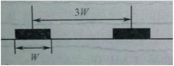
3W Rule
In order to reduce crosstalk between lines, the line spacing should be large enough. When the line center spacing is not less than 3 times the line width, 70% of the electric field can be maintained without mutual interference, which is called the 3W rule. To achieve a 98% electric field that does not interfere with each other, a spacing of 10W can be used.
In actual PCB design, the 3W rule cannot completely meet the requirement of avoiding crosstalk.
According to practical experience, if there is no shielding ground, printed above is greater than the LCM distance between signal lines to prevent crosstalk, well so in PCB circuit wiring, requires the noise signals (such as the clock line) and the noise signal, and EFTlB, ESD interference such as the "dirty" and "clean" need to be protected in line, not only to be forced to use 3w rules but also for shielding ground packet processing, in order to prevent the happening of the crosstalk.

In addition, to avoid crosstalk in PCB, PCB design and layout should be considered, for example
1. Classify logic device series according to function, and keep bus structure strictly controlled.
2. Minimize the physical distance between components.
3. High-speed signal lines and components (such as crystal oscillators) should be kept away from interconnection interfaces and other areas susceptible to data interference and coupling.
4. Provide correct terminals for high-speed lines.
5. Avoid long-distance parallel wiring, and provide sufficient spacing between wiring to minimize inductive coupling.
6. Wiring on adjacent layers (microstrip or strip) should be perpendicular to each other to prevent capacitance coupling between layers.
7. Reduce the distance between the signal and the ground plane.
8. Separate and isolate high-noise emission sources (clock, I/O, high-speed interconnection), and different signals are distributed in different layers.
9. Increase the distance between signal lines as much as possible, which can effectively reduce capacitive crosstalk.
10. Reduce the lead inductance, avoid using load with very high impedance and load with very low impedance in the circuit, and try to keep the load impedance of the analog circuit stable between loQ ~ lokQ.Because a high impedance load will increase capacitive crosstalk when a very high impedance load is used, capacitive crosstalk will increase due to high operating voltage, while when a very low impedance load is used, inductive crosstalk will increase due to high operating current.
11. Lay high-speed periodic signals on the inner layer of PCB.
12. Use impedance matching technology to ensure the integrity of the BT signal and prevent overshoot.
13. Pay attention to the signal with a fast-rising edge (tr≤3ns), carry out ground anti-crosstalk processing and arrange some signal lines disturbed by EFTlB or ESD and not filtered on the edge of PCB.
14. Use the ground plane as much as possible. The signal line using the ground plane will get 15 ~ 20dB attenuation compared with the signal line not using the ground plane.
15. Signal high-frequency PCB signal and sensitive signal are included in the ground processing, and the attenuation of 10 ~ 15dB will be obtained by using the ground covering technology in the double panel.
16. Use a balanced line, shield line, or coaxial line.
17. Filter harassment signal line and sensitive line.
18. Reasonable setting of layers and wiring, reasonable setting of wiring layers and wiring spacing, reduction of the length of parallel signals, reduction of the spacing between signal layers and plane layers, an increase of the spacing between signal lines, and reduction of the length of parallel signal lines (within the key length range) can effectively reduce crosstalk.

Conditions for the establishment of the 3W rule
Although the 3W rule is easy to remember, it should be emphasized that there are prior conditions for its establishment.
Considering the physical significance of the cause of crosstalk, to effectively prevent crosstalk, the spacing is related to the stack height and wire width.
For the 4-layer PCB board, 3W is enough for the distance between the routing and the reference plane height (5~10mils);
However, for two-layer boards, the distance between the routing and the reference layer height (45~55mils), 3W may not be enough for high-speed signal routing.
The 3W rule generally holds under the condition of 50ohm characteristic impedance transmission line.
The 3W rule means that when multiple high-speed signal lines are routed for a long distance, their spacing should follow the 3W rule, such as clock lines, differential lines, video and audio signal lines, reset signal lines and other key circuits of the system need to follow the 3W rule, but not all wiring on the board must be forced to comply with the 3W rule.