Distinguishing quality of the interface circuit board (Normally, the appearance of the PCB circuit board can be analyzed and judged by three points;
1. The standard rules for size and thickness.
The thickness of the circuit board with the circuit board standards that differ in size, customers can measure and inspect in accordance with the thickness of their own products and specifications.
2. Light and color.
the external circuit board covered with ink, the circuit board can play the role of insulation, if the board is not bright colors, less ink, insulation board itself is not good.
3. Appearance welding.
circuit board as part of a more, if welding is not good, easy to fall portion of the circuit board, seriously affecting the quality of the circuit board welding, good appearance, carefully identified, the interface is very important.
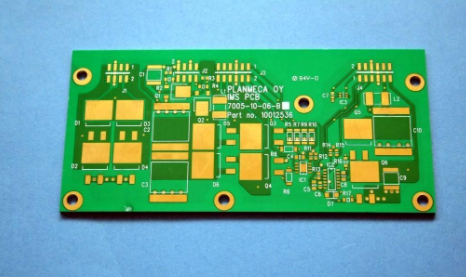
PCB prototype includes high-frequency PCB, rigid-flex PCB and multi-layer PCB fabrication.
High-frequency PCB is a special PCB prototype with high electromagnetic frequency. Generally speaking, the working frequency of high-frequency PCB is above 1GHz. Its precision and technical parameters requirements are very high, commonly used in automotive anti-collision systems, satellite systems, radio systems, radar systems, instruments and other fields.
PCB prototype produced by iPCB includes:
Rogers PCB series, Arlon PCB series, Taconic PCB series, nelco PCB series, isola PCB(isola 370hr, isola fr408) and Teflon PCB, PTFE PCB, ceramic PCB, hydrocarbon PCB, hybrid PCB, ic substrate, ic test board, high-speed PCB.
PCB prototype fabrication capacity of iPCB:
PCB thickness: 0.10-8.0mm(1layer and 2layers) 0.15 -8.0mm(Multi-Layers), Min finish board size: 0.5*1.0mm, High Frequerncy mixed pressure layers: 4-32layers, For more details, please click: High Frequency Hybrid board technical Capacity.

PCB prototype
Advantages of Rigid-Flex PCB: Rigid-Flex PCB has the characteristics of FPC Prototype and PCB Prototype at the same time. Therefore, it can be used in some products with special requirements, which not only has a certain flexible area, but also has a certain rigid area, which is of great help to save the internal space of the product, reduce the volume of the finished product, and improve the product performance.
Disadvantages of Rigid-Flex PCB: at present, the production process of Rigid-Flex PCB Prototype is various, the production is difficult, the yield rate is low, and there are many materials and manpower. Therefore, the price of Rigid-Flex PCB Prototype is relatively expensive and the production cycle is relatively long.
With the development of VLSI, miniaturization and high integration of electronic components, Multi-layer PCB Prototype is moving towards the direction of matching with high-function circuits. Therefore, the demand for high-density lines and high-capacity wiring is increasing, and the requirements for electrical characteristics (such as the integration of crosstalk and impedance characteristics) are becoming more and more strict. The popularity of multi pin parts and surface mount components (SMD) makes the shape of PCB circuit pattern more complex, the conductor circuit and aperture smaller, and the development of high-level Multi-layer PCB Prototype (10-70 layers). In order to meet the requirements of small.
IC Substrate is also called packaging substrate. In the field of high-level packaging, IC Substrate has replaced the traditional lead frame and become an indispensable part of chip packaging. It not only provides support, heat dissipation and protection for the chip, but also provides electronic connection between the chip and PCB motherboard; Even passive and active components can be embedded to achieve certain system functions.
IC Substrate is a technology developed with the continuous progress of semiconductor packaging technology. In the mid-1990s, a new type of IC high-density packaging represented by ball grid array packaging and chip size packaging came out. As a new packaging carrier, IC carrier board was born.
IC Substrate is developed on the basis of HDI board. As a high-end PCB board, it has the characteristics of high density, high precision, miniaturization and thinness.
ipcb has been able to produce BGA and EMMC IC Substrate PCB prototype.