Bumping technology has been widely used in the semiconductor industry, and more and more professional wafer manufacturers use it to replace traditional electroplating soldering or high-precision solder paste printing processes. Since direct ball implantation provides a flexible, fast, accurate and low-cost solution for secondary assembly, large EMS companies have gradually entered this field.

OEM customers have accepted the new concept in device manufacturing, that is, devices can be manufactured in EMS companies and used directly in the assembly of final products. The benefits of doing this are: it provides a higher rate of return, shortens the product delivery time, meets the requirements of small and medium batches, and more importantly reduces costs. Under this situation, it is becoming more and more necessary for the smt industry to apply ball implantation technology, and EMS companies can only respond to the requirements of OEM customers if they have mastered wafer-level and chip-level packaging technologies.
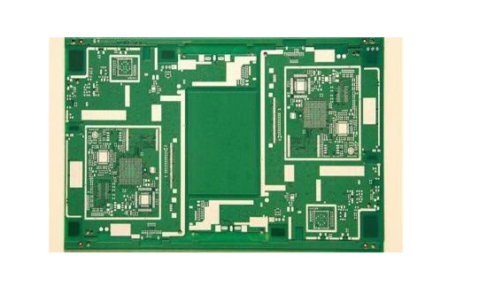
This article mainly introduces the ball planting technology applied on the circuit board.
Introduction to the process
The whole process includes four steps: applying flux, planting balls (ball printing), inspection and rework, and reflow soldering.
Ball planting requires two online printers: one is an ordinary screen printing machine for applying paste flux, and the other is for planting balls (using a special planting printing head). Both printing presses can be switched to ordinary printing presses for electronic assembly at any time. In addition, the low-cost equipment used to rework balls before the furnace can effectively avoid quality problems such as fewer balls.
Step 1: Coating Flux Coating paste flux is a step of the ball planting process, it is a key step to maintain the positioning of the ball and to form a good shape in the reflow soldering. A specially designed screen is used for the printing of paste flux. The opening of the screen is determined based on the size of the printed circuit board's pad and the size of the solder balls.
In the step of printing paste flux, two types of squeegees are used at the same time. The front squeegee is a rubber squeegee (Figure 2) and the rear squeegee is a metal vertical squeegee.The vertical squeegee first coats a thin layer of flux evenly on the screen, and then the rubber squeegee prints the flux on the circuit board pads. The advantage of this process design is to provide a flat and uniform flux layer on the pads of the circuit board, while also keeping the screen wet and not dry, effectively preventing the flux from blocking the holes.
DOE is used to determine the best parameters for flux printing.
After printing, observe and calculate the coverage of the flux on the pad with a microscope, and calculate the result of DOE. Table 2 is the DOE matrix data of actual flux printing.
Flux coverage rate reflects the results of DOE experiment. the one is an example of flux printing defects, including printing misalignment, excessive overflow, and low volume.
From the analysis of the influence diagram of the main relationship between the various factors and the cross-linking reaction, the printing speed, printing pressure, squeegee angle and printing gap have a significant influence on the flux printing result, and the cross-linking between the various factors The same goes for the joint reaction.
Based on the parameter matrix optimization analysis, the optimized parameter settings can be obtained, as shown in Table 3.
In this DOE experiment, optimized printing parameter settings can be obtained; of course, different equipment will have certain differences. In the production process, the stencil is easily damaged, so it needs to be handled and moved carefully. In the process of flux printing, solid dust or other foreign substances can easily block the opening of the screen, which can only be cleaned with an air gun. Cleaning agents such as isopropyl alcohol or alcohol can not be used to clean the screen, because it will dissolve and destroy the polymer material on the screen. Usually, after the production is finished, wipe it with a dust-free cloth dampened with deionized water and dry it with an air gun.
After the flux printing is completed, it is necessary to check under a microscope for missing printing, insufficient quantity or misalignment. Usually the flux is transparent, and it is difficult to detect defects by visual inspection. To facilitate visual inspection, it is necessary to change the color of the flux reasonably.
Step 2: Plant the ball
In the ball planting stage, a specially designed template is also required. The opening design of the template is also based on the actual size of the solder balls and the size of the circuit board pads. This is based on two considerations: one is to prevent the flux from contaminating the template and the solder balls; the other is how to make the solder balls pass through the template smoothly Open up.
The template structure has two layers: the main body is an electroformed template, which has a smoother hole wall than a laser or chemically etched template, so that the solder balls can pass smoothly; the second layer is a slightly flexible isolation that is tightly bonded to the bottom of the template Layer.The two composite layers have almost the same thickness as the diameter of the solder ball, which prevents the paste flux from contaminating the electroforming template, and at the same time allows the solder ball to pass through the template to the pad and be stuck by the flux.
The specially designed ball planting printing head can make the friction between each solder ball and the template reach low, and apply a controllable placement force to put the solder ball into each opening (the solder ball is through capillary action and The influence of gravity is distributed to each opening). In this step, the solder ball transfer equipment is extremely critical, and the parameter definitions for solder ball printing are shown in Table 4.
Occasionally, solder ball plugging occurs during the printing process, which is caused by the plugging of the openings with fine dust or fibers. Because it is difficult to determine which solder ball is damaged, it is necessary to scrap all the solder balls to be printed, so the solder ball rejection rate is relatively high.
In this step, the template does not need to be cleaned. IPA or alcohol cleaners cannot be used to wipe the template, because organic cleaners will destroy the adhesion between the two layers of the template. If clogging occurs, you can use an air gun to clean it.
Step 3: Inspection and rework
AOI (Automatic Optical Inspection) equipment is used for online inspection after ball planting. The main defects are usually fewer balls and misalignment (see Figure 9). After inspection, the circuit board with fewer balls needs to be reworked with offline semi-automatic ball filling equipment; for misalignment defects, cleaning the circuit board and reprinting is the only way.
The offline semi-automatic ball filling equipment is specially designed for the replanting of the few balls. The placement of the few balls requires the use of an accurate image magnification system. First, use an operating arm to apply paste flux on the ball-missing pads, and then use Another operating arm fills up the ball on the pad. If the flux on the pad is already sufficient, the step of applying flux can be omitted when writing the program. Interstitial air pressure control is the key to complete flux coating and ball filling. Figure 10 shows the structure of the ball-filling device.
The offline ball filling equipment is very important, and it should not affect other accurately placed solder balls on the circuit board. After rework, the circuit board needs to be re-checked with AOI equipment before reflow soldering to ensure that there is no defect.
Step 4: Reflow soldering
The reflow soldering process of ball planting is the same as the ordinary smt reflow soldering process. For lead-free products, the generally used solder alloy is SAC105, which has a slightly higher melting point than lead-free solder paste used for circuit boards(usually 2 to 3°C higher) to prevent defects from being caused again in the secondary reflow. Of course, this also depends on the customer's process regulations. Fig. 11 is a graph of reflow soldering of the ball planting.
AOI inspection is required after reflow soldering. In this step, considering that the product is actually a BGA type, if there are any missing balls or misalignment, the circuit board will be scrapped, because any way of repair may cause component failure in the next assembly process.
summary
This research on the ball planting process is to find the standard process of coating flux, planting ball, rework and reflow soldering from the perspective of EMS company's production. The key points in the research are the setting of flux coating parameters, the ball placement template and the rework of missing solder balls. The research also found that there is a problem of insufficient detectability in the inspection after the paste flux printing; therefore, it is necessary to cooperate with the flux supplier to seek further research that is beneficial to the inspection effect after printing.
The above is an introduction to the application of ball planting technology in the SMT industry.