Causes and prevention of smt tin beads

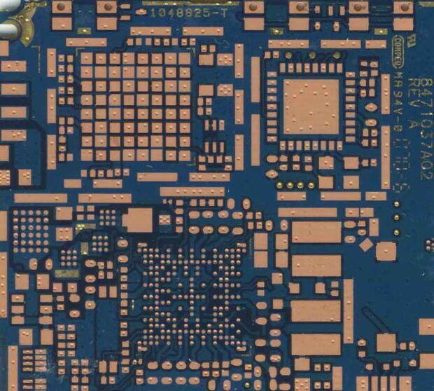
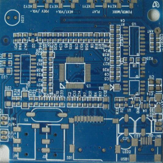
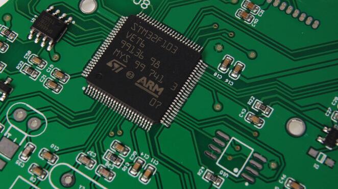
Today, with the rapid development of smt technology in Kunshan, the manufacturing of products is developing towards miniaturization and integration. But until today, some disturbing problems often occur in the manufacturing of Kunshan smt. It is more common to have small tin bead problems next to the mounted components.
This article proposes discussion and suggestions on the occurrence of tin beads and countermeasures.
1. The cause of the solder beads next to the component
Solder paste is squeezed due to excessive mounting pressure during printing and component placement. When entering the reflow furnace for heating, the temperature of the component usually rises faster than that of the PCB board, while the temperature below the component rises more slowly. Then, the soldering end of the component comes into contact with the solder paste, and the viscosity of the Flux decreases due to the increase in temperature, and it climbs closer due to the higher temperature above the component conductor. Therefore, the solder paste starts to melt from the outside of the high temperature pad.
The molten solder begins to extend upward from the soldering end of the component to form a solder joint. Then the flux moves in the unmelted solder, and the flow of the flux is blocked by the molten solder, so the flux cannot flow out. The generated volatile solvent (GAS) also blocks the coating due to the melting of the solder.
3, The melting direction of the solder paste progresses toward the inside of the pad, the Flux is also squeezed inward, and the (GAS) is also inward
move. Under the component a. point, due to the moving force of the Flux, the molten solder reaches the point b., and the point a. stops falling due to poor tin eating, resulting in a backflow of force at the point c. The resulting solder is squeezed out, resulting in tin beads.
B Improvement measures
1. The pad design should consider the uniform temperature rise during the soldering process to ensure temperature balance. On this basis, the size and dimensions of the pad are determined. At the same time, it is necessary to consider the matching between the height of the component and the area of the pad, so that the melted solder retains a stretch of space.
2. Soldering reflow temperature curve should not rise sharply.
3. Control of printing accuracy and printing volume, and management during printing. Prevent solder paste printing offset or poor soldering. (More tin, shape collapse)
4. Pressure adjustment of mounting components. Avoid components that squeeze the solder paste out of shape.
5. The quality of the component itself, to avoid oxidation regain.
The above is an introduction to the causes and prevention of SMT solder beads. Ipcb also provides PCB manufacturers and PCB manufacturing technology.