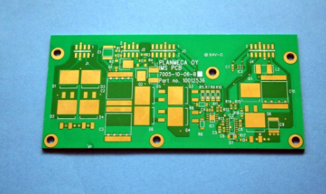
1. Layout of components on smt-PCB

1. When the circuit board is placed on the conveyor belt of the reflow soldering furnace, the long axis of the component should be perpendicular to the transmission direction of the equipment, so as to prevent the component from drifting or "tombstone" phenomenon on the board during the soldering process.
2. The components on the PCB should be evenly distributed, especially the high-power components should be dispersed, to avoid local overheating on the PCB when the circuit is working, which will affect the reliability of the solder joints.
3. For double-sided mounting components, the larger components on both sides should be installed in a staggered position, otherwise the welding effect will be affected due to the increase of local heat capacity during the welding process.
4, PLCC/QFP and other components with pins on four sides cannot be placed on the wave soldering surface.
5. The long axis of the large smt device installed on the wave soldering surface should be parallel to the direction of solder wave flow, so as to reduce the solder bridging between the electrodes.
6. The large and small smt components on the wave soldering surface cannot be lined up in a straight line and should be staggered to prevent false soldering and missing soldering due to the "shadow" effect of the solder wave crest during soldering.
Two, the pad on the smt-PCB
1. For smt components on the wave soldering surface, the pads of larger components (such as transistors, sockets, etc.) should be appropriately enlarged. For example, the pads of SOT23 can be lengthened by 0.8-1mm, which can avoid the "shadow effect due to components" "The resulting empty welding.
2. The size of the pad should be determined according to the size of the component. The width of the pad is equal to or slightly larger than the width of the electrode of the component, and the welding effect is good.
3. Between two interconnected components, avoid using a single large pad, because the solder on the large pad will connect the two components to the middle. The correct way is to separate the pads of the two components, Use a thinner wire to connect between the two pads. If the wire is required to pass a larger current, several wires can be connected in parallel, and the wires are covered with green oil.
4. There should be no through holes on or near the pads of smt components. Otherwise, during the REFLOW process, the solder on the pads will flow away along the through holes after melting, resulting in false soldering, less tin, or flow Causes a short circuit to the other side of the board.
The above is an introduction to the design principles of SMT-PCB. Ipcb is also provided to PCB manufacturers and PCB manufacturing technology