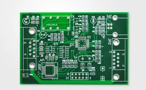
Welding is actually a chemical treatment process. A printed circuit board(PCB) is a support for circuit elements and devices in electronic products, and it provides electrical connections between circuit elements and devices. With the rapid development of electronic technology, the density of PCB is getting higher and higher, and there are more and more layers. Sometimes all the designs may be correct (such as the circuit board is not damaged, the printed circuit design is perfect, etc.), but because of the There are problems in the welding process, which lead to welding defects and deterioration of welding quality, which affects the pass rate of the circuit board, which in turn leads to the unreliable quality of the whole machine. Therefore, it is necessary to analyze the factors that affect the welding quality of the printed circuit board, analyze the reasons for the welding defects, and improve the welding quality of the entire circuit board.

Causes of welding defects
1. PCB design affects soldering quality
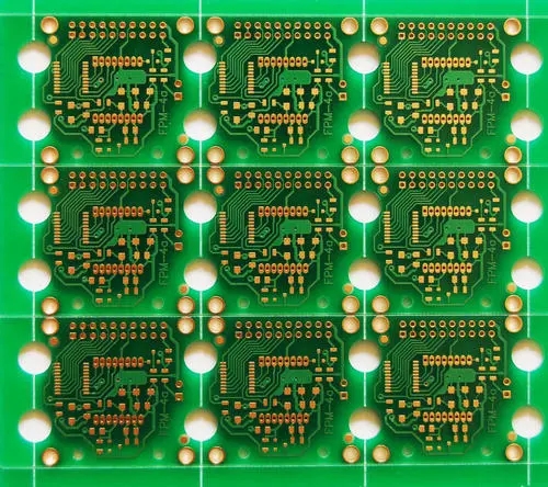
In terms of layout, when the PCB size is too large, although the soldering is easier to control, the printed lines are long, the impedance increases, the anti-noise ability is reduced, and the cost increases; Interference, such as electromagnetic interference of circuit boards. Therefore, the PCB board design must be optimized: (1) Shorten the wiring between high-frequency components and reduce EMI interference. (2) Components with heavy weight (such as more than 20g) should be fixed with brackets and then welded. (3) The heat dissipation problem should be considered for heating elements to prevent defects and rework caused by large ΔT on the surface of the element, and the thermal element should be far away from the heat source. (4) The arrangement of the components is as parallel as possible, which is not only beautiful but also easy to weld, and is suitable for mass production. The circuit board is preferably designed as a 4:3 rectangle. Do not change the wire width to avoid wiring discontinuities. When the circuit board is heated for a long time, the copper foil is easy to expand and fall off. Therefore, avoid using large-area copper foil.
2, the solderability of the circuit board hole affects the soldering quality
The solderability of the circuit board hole is not good, it will produce virtual soldering defects, which will affect the parameters of the components in the circuit, resulting in unstable conduction of the multi-layer board components and the inner line, causing the entire circuit to fail. The so-called solderability is the property that the metal surface is wetted by molten solder, that is, a relatively uniform continuous smooth adhesion film is formed on the metal surface where the solder is located. The main factors that affect the solderability of printed circuit boards are: (1) The composition of the solder and the nature of the solder. Solder is an important part of the welding chemical treatment process. It is composed of chemical materials containing flux. Commonly used low-melting eutectic metals are Sn-Pb or Sn-Pb-Ag. The impurity content must be controlled by a certain proportion to prevent the oxides generated by the impurities from being dissolved by the flux. The function of the flux is to help the solder wetting the surface of the circuit to be soldered by transferring heat and removing rust. White rosin and isopropanol solvents are generally used. (2) The welding temperature and the cleanliness of the metal plate surface will also affect the weldability. If the temperature is too high, the solder diffusion speed will increase. At this time, it will have a high activity, which will cause the circuit board and the molten surface of the solder to oxidize rapidly, resulting in soldering defects. Contamination on the surface of the circuit board will also affect the solderability and cause defects. These defects Including tin beads, tin balls, open circuits, poor gloss, etc.
3, welding defects caused by warpage
PCB and components warp during the welding process, and defects such as virtual welding and short circuit due to stress deformation. Warpage is often caused by the temperature imbalance of the upper and lower parts of the PCB. For large PCBs, warping will also occur due to the drop of the board's own weight. The ordinary PBGA device is about 0.5mm away from the printed circuit board. If the device on the circuit board is larger, the solder joint will be under stress for a long time as the circuit board cools down and the solder joint will be under stress. If the device is raised by 0.1mm, it will be enough to cause Weld open circuit.
While the PCB warps, the components themselves may also warp, and the solder joints located in the center of the components are lifted away from the PCB, resulting in empty soldering. This situation often occurs when only flux is used and no solder paste is used to fill the gap. When using solder paste, due to deformation, the solder paste and the solder ball are connected together to form a short circuit defect. Another reason for the short circuit is the delamination of the component substrate during the reflow process. This defect is characterized by the formation of bubbles under the device due to internal expansion. Under X-ray inspection, it can be seen that the welding short circuit is often in the middle of the device. .