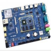
In the design and manufacturing process of high-speed PCB circuit boards, engineers need to start with wiring and component settings to ensure that this PCB board has good signal transmission integrity. In today's article, we will introduce some wiring techniques often used in PCB signal integrity design for newcomers engineers, hoping to bring some help to newcomers' daily study and work.

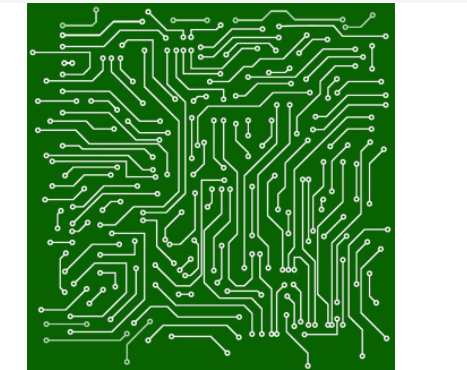
In the design process of high-speed PCB circuit boards, the cost of the printed circuit of the substrate is proportional to the number of layers and the surface area of the substrate. Therefore, under the premise of not affecting the system function and stability, engineers should use as few layers as possible to meet the actual design needs, which will inevitably increase the wiring density. In the PCB wiring design, the greater the wiring width Fine, the smaller the interval, the greater the crosstalk between signals, and the smaller the transmission power. Therefore, the selection of trace size must consider various factors.
In the PCB layout design process, the principles that engineers need to follow are mainly as follows:
First of all, designers should minimize the bending of the leads between the pins of the high-speed circuit devices during the wiring process, and use 45? fold lines to reduce the external reflection and mutual coupling of high-frequency signals.
Secondly, when performing PCB board wiring operations, designers try to shorten the lead between the pins of the high-frequency circuit device and the inter-layer alternation of the leads between the pins as much as possible. High-frequency digital signal traces should be as far away as possible from analog circuits and control circuits.
In addition to the precautions for PCB wiring mentioned above, engineers also need to be cautious when dealing with differential signals. Because the differential signal has the same amplitude and the same direction, the magnetic fields generated by the two signal lines cancel each other out, which can effectively reduce EMI. The spacing of the differential lines often leads to changes in the differential impedance, and the inconsistency of the differential impedance will seriously affect the signal integrity. Therefore, in actual differential wiring, the length difference between the two signal lines of the differential signal must be controlled at the time of the rising edge of the signal. Within 20% of the electrical length. If conditions permit, the differential wiring must meet the back-to-back principle and be in the same wiring layer. In the setting of the line spacing of differential wiring, engineers need to ensure that it is at least equal to or greater than 1 times the line width. The distance between differential traces and other signal lines should be greater than three times the line width.