1. Background introduction
With the development of PCB functionalization and high performance, high-end fine products such as high-frequency and high-speed PCB, high heat dissipation PCB, buried resistance and buried capacitance PCB board have gradually become well-known in the industry, and the development of PCB has shown diversification. On the one hand, due to market demand, customers’ designs tend to be open and bold, and PCB products with many special requirements have emerged; on the other hand, new materials, new equipment, and new processes have emerged to cater to the market. And the needs of customers for product features.

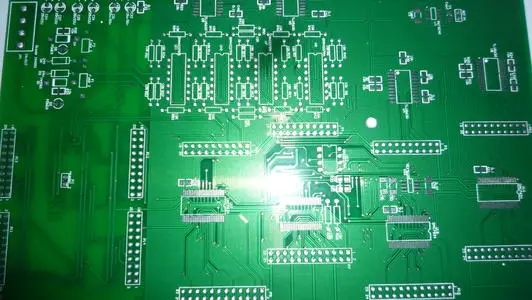
According to the requirements of a customer, our company produces a product that realizes the precise resistance control (16±10Ω) requirements of the established wiring method on the PCB. The customer data only gives the total trace length (6413mm), and the line width is required to be about 0.2mm, but it is not strictly required. Appropriate adjustment is allowed. It is necessary for our company to calculate the matching line width and copper thickness range according to the actual process capability., And then produce PCB products that meet the impedance requirements.
2. Theoretical calculation
The design pattern of the customer's resistance control board only has a long resistance line on the BOT surface. The bus length is 6413mm. The line width is calculated as 0.2mm in advance. The TOP surface is 0.4mm wider and the line length is 15.8mm. The resistivity of copper is calculated according to the theoretical value of 1.75*10-8Ω*m, and the control resistance is 16+/-10Ω. According to the theoretical calculation, it is assumed that the thickness of the finished copper is 1OZ, the BOT surface resistance is 15.36Ω, and the T OP resistance is about 0.02Ω. It is estimated that the resistance control surface is only the BOT surface.
The theoretical calculation value of the resistance of a 6413mm long and 0.2mm wide copper wire under different copper thicknesses is shown in the table below. R=ρ*L/S, ρ is the material resistivity 1.75*10-8Ω*m, L is the wire length 6413mm, S is the cross-sectional area of the wire, the upper and lower limits of the actual resistance are 17.6Ω and 14.4Ω respectively. Theoretical calculation is that when the copper thickness is 35um, a wire with a width of 0.2mm and a length of 6413mm can reach the ideal resistance value of 16Ω.
The actual production of surface copper is controlled at about 35um. The hole copper requirement of this board is smaller than 18um. Considering the thickness of the board is 0.5mm, the hole diameter is 0.35mm, the drilling thickness-to-diameter ratio is about 1.4, the electroplating hole rate is calculated at 90%, and the surface copper electroplating layer The thickness is at least about 20um, so the bottom copper should be 35um-20um=15um, and the copper plating thickness from 1/3oz is ideal.
If the median value of the surface copper control is 35um, the actual copper thickness is between 30 and 40um. According to the customer's resistance requirements, the calculated line width tolerance range is as shown in Table 2. According to the calculation results of the table below, control the theoretical optimal range of copper thickness from 32 to 40um. between.
The actual design of the PCB production process is positive, which is more convenient for line width tolerance control, and more precise resistance is obtained.
Three, process control
3.1 Copper behind the board
The thickness of the board electrical copper is 8um. After the actual board electrical measurement, the surface copper of the 2PNL board is measured. After the measurement, the copper thickness distribution Cpk is calculated to be 1.4>1.33. As shown in Table 3, the electrical uniformity of the board is ideal.
3.2 The copper thickness of the finished product after the figure is electrified
The actual value of the copper surface copper of the slice measuring hole is about 24um, and the copper thickness of the surface copper is about 35 to 39um, and the copper thickness is qualified.
3.3 Line width resistance record after etching
On the test board 2PNL, the average line width of PNL1 is 0.19mm by etching, and the measured resistance is between 15.8 and 19Ω; the average line width of PNL2 is 0.21mm, and the measured resistance is between 15.2Ω and 17.5Ω. The first time I did it, I was not sure how much the process would affect the resistance, so I continued to follow up the resistance test results from the test board to the finished product.
3.4 Finished resistance test
The test resistance of the finished product is shown in Table 5. The resistance of the 2PNL board is all qualified, but compared to the etched semi-finished product, the resistance of the finished product is reduced by 1.5 ohms.
Fourth, the conclusion
All resistances measured on the finished test board are qualified, indicating that the board electrical copper thickness is controlled at 21+/-3um, the finished copper thickness is controlled at an average of 35um to more than 40um, the line width is controlled between 0.19 and 0.21, and the finished resistance is qualified. And the resistance of the semi-finished product after etching is about 1.5Ω larger than that of the finished product. Therefore, theoretically, the etching measurement resistance should be pre-larged to 1.5Ω. The pre-sizing has a considerable relationship with the difference caused by the PCB design and solder mask and surface treatment process. The resistance pre-sizing of different PCBs after etching needs to take these factors into consideration.
The influencing factors that cause the difference between the resistance of the semi-finished product after etching and the resistance of the finished product include post-process micro-etching, whether the wire is covered with oil, and whether the wire is subjected to other surface treatments. The resistance of the surface treatment layer as a parallel resistance requires special consideration, especially nickel sinking. For gold, electro-nickel gold, etc., the surface treatment layer itself is a conductor, and its resistance is not negligible compared to the resistance of copper wires. Therefore, in general, in order to facilitate the control, it is recommended that the wire layer of the control resistor be directly covered with oil to avoid large resistance errors in the subsequent process.