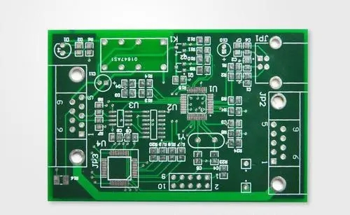
For switch-mode converters, an excellent printed circuit board(PCB) layout is essential to obtain good system performance. If the PCB design is improper, it may cause the following consequences: too much noise to the control circuit and affecting the stability of the system; too much loss on the PCB traces and affecting the system efficiency; too much electromagnetic interference and affecting the compatibility of the system sex.

ZXLD1370 is a multi-topology switch mode LED driver controller, and external switching devices are embedded in each different topological structure. The LED driver is suitable for buck, boost or buck-boost mode.
This article will take the ZXLD1370 device as an example to discuss the considerations of PCB design and provide relevant suggestions.
Consider the trace width
For switch-mode power circuits, the main switch and related power devices carry large currents. The traces used to connect these devices have resistances related to their thickness, width, and length. The heat generated when current flows through the trace will not only reduce efficiency, but also increase the temperature of the trace. In order to limit the temperature rise, it is important to ensure that the trace width is sufficient for the rated switching current.
The following equation shows the relationship between the temperature rise and the cross-sectional area of the trace.
Internal trace: I=0.024*dT0.44*A0.725
External trace: I=0.048*dT0.444*A0.725
Among them: I=large current (A); dT=temperature rise above the environment ( degree Celsius); A=cross-sectional area (mil2).
For switch-mode power converter applications designed with surface mount devices, the copper surface on the PCB can also be used as a heat sink for power devices. The temperature rise of the trace caused by the conduction current should be reduced to a low level. It is recommended to limit the temperature rise of the trace to less than 5oC.
The above is the introduction of optimizing the PCB layout to improve the performance of the converter. Ipcb is also provided to PCB manufacturers and PCB manufacturing technology