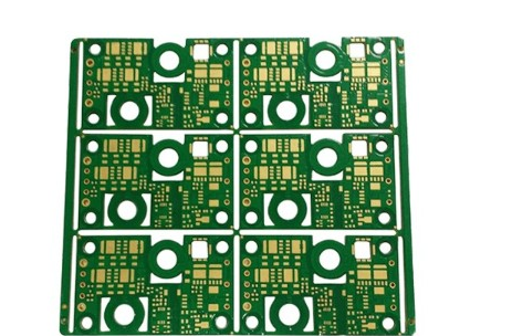
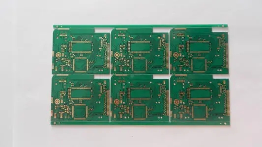
The manufacturing process of printed circuit boards

Let's take a look at how a printed circuit board is made, taking four layers as an example.
Four-layer PCB board production process:
1. Chemical cleaning-【Chemical Clean】
In order to obtain good-quality etching patterns, it is necessary to ensure that the resist layer is firmly bonded to the substrate surface, and the substrate surface is required to be free of oxide layers, oil stains, dust, fingerprints and other dirt. Therefore, before coating the resist layer, the surface of the board must be cleaned and the surface of the copper foil must reach a certain degree of roughness.
Inner board: start to make four-layer board, the inner layer (two and three layers) must be done first. The inner plate is a copper sheet compounded on the upper and lower surfaces by glass fiber and epoxy resin.
2. Cut Sheet Dry Film Lamination-【Cut Sheet Dry Film Lamination】
Coating photoresist: In order to make the shape we need for the inner plate, we first paste a dry film (photoresist, photoresist) on the inner plate. The dry film is composed of polyester film, photoresist film and polyethylene protective film. When attaching the film, first peel off the polyethylene protective film from the dry film, and then paste the dry film on the copper surface under heating and pressurizing conditions.
3. Exposure and development-[Image Expose] [Image Develop]
Exposure: Under the irradiation of ultraviolet light, the photoinitiator absorbs the light energy and decomposes into free radicals. The free radicals then initiate the polymerization and crosslinking reaction of the photopolymerized monomers, and form a polymer structure insoluble in dilute alkali solution after the reaction. The polymerization reaction will continue for a period of time. To ensure the stability of the process, do not tear off the polyester film immediately after exposure. It should stay for more than 15 minutes to allow the polymerization reaction to continue. Tear off the polyester film before developing.
Development: The active groups in the unexposed part of the photosensitive film react with the dilute alkali solution to produce soluble substances and dissolve, leaving the pattern part that has been photosensitive, cross-linked and cured.
4. Etching-[Copper Etch]
In the production process of flexible printed boards or printed boards, the unnecessary part of the copper foil is removed by a chemical reaction method to form the required circuit pattern, and the copper under the photoresist is retained and not etched Of the impact.
5. Film removal, punching after etching, AOI inspection, oxidation
Strip Resist] [Post Etch Punch] [AOI Inspection] [Oxide]
The purpose of film removal is to remove the resist layer remaining on the board surface after etching to expose the copper foil underneath. "Membrane residue" filtration and waste liquid recovery must be properly handled. If the water washing after removing the film can be completely cleaned, you can consider not to do pickling. After cleaning the surface of the board, it must be completely dry to avoid residual moisture.
6. Layup-protective film film【Layup with prepreg】
Before entering the laminator, the raw materials for each multilayer board need to be prepared for Lay-up operation. In addition to the oxidized inner layer, a protective film film (Prepreg)-epoxy resin impregnated glass is required fiber. The function of the lamination is to stack the boards covered with the protective film in a certain order and place them between the two-layer steel plates.
7. Laminated board-copper foil and vacuum lamination
【Layup with copper foil】【Vacuum Lamination Press】
Copper foil-Cover the current inner sheet with a layer of copper foil on both sides, and then perform multi-layer pressure (extruding that requires temperature and pressure to be measured in a fixed time) and cool to room temperature after completion, and the rest It is a multi-layer board.
8.CNC Drilling【CNC Drill】
Under the precise conditions of the inner layer, CNC drilling is drilled according to the pattern. The drilling accuracy is very high to ensure that the hole is in the correct position.
9. Electroplating-Through Hole【Electroless Copper】
In order for the through holes to be conductive between the layers (to metalize the resin and glass fiber bundles on the non-conductor part of the hole wall), the holes must be filled with copper. The first step is to plate a thin layer of copper in the hole. This process is completely chemical. The thickness of the final copper plating is one millionth of 50 inches.
10. Cut Sheet [Cut Sheet] [Dry Film Lamination]
Apply photoresist: We once applied photoresist on the outer layer.
11. Exposure and development-[Image Expose] [Image Develop]
Outer layer exposure and development
12. Line electroplating: [Copper Pattern Electro Plating]
This time it has also become a secondary copper plating, and the main purpose is to thicken the copper thickness of the circuit and the through-hole.
13. Tin Pattern Electro Plating [Tin Pattern Electro Plating]
Its main purpose is to etch resist to protect the copper conductor it covers from being attacked during alkaline copper etching (to protect all copper lines and the inside of through holes).
14. Strip Resist【Strip Resist】
We already know the purpose, and only need to use chemical methods to expose the copper on the surface.
15. Etching【Copper Etch】
We know the purpose of the etching, and the tin-plated part protects the copper foil underneath.
16. Pre-hardening, exposure, development, upper solder mask
[LPI coating side 1] [Tack Dry] [LPI coating side 2] [Tack Dry]
[Image Expose] [Image Develop] [Thermal Cure Soldermask]
The solder mask layer is used to expose the pads, which is commonly referred to as the green oil layer. In fact, holes are dug in the green oil layer to expose the pads and other places that do not need to be covered with green oil. Proper cleaning can get the proper surface characteristics.
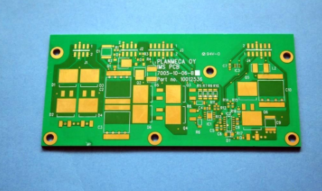
17. Surface treatment
【Surface finish】
> HASL, Silver, OSP, ENIG hot air leveling, immersion silver, organic solder protection agent, chemical nickel gold
> Tab Gold if any gold finger
The hot air leveling solder coating HAL (commonly known as spray tin) process is to dip the printed board with flux, then dip it in the molten solder, and then pass between the two air knives, using the hot compression in the air knives The air blows off the excess solder on the printed board and at the same time removes the excess solder in the metal hole, thereby obtaining a bright, smooth and uniform solder coating.
The purpose of gold finger (or Edge Connector) design is to use the connector of the connector as the outlet of the board to connect to the outside, so the gold finger manufacturing process is required. The reason why gold is selected is because of its superior conductivity and Oxidation resistance. But because of the high cost of gold, it is only used for gold fingers, partial plating or chemical gold
After summarizing all the processes:
1) Inner Layer
> Chemical Clean
> Cut Sheet Dry Film Lamination
> Image Expose
> Image Develop
> Copper Etch
> Strip Resist
> Post Etch Punch
> AOI Inspection
> Oxide
> Layup stack
> Vacuum Lamination Press
2) CNC Drilling
> CNC Drilling
3) Outer Layer
> Deburr
> Etch back-Desmear
> Electroless Copper Plating-Through Hole
> Cut Sheet Dry Film Lamination
> Image Expose
> Image Develop
4) Plating
> Image Develop
> Copper Pattern Electro Plating
> Tin Pattern Electro Plating
> Strip Resist
> Copper Etch
> Strip Tin
5) Solder Mask
> Surface prep
> LPI coating side 1 printing
> Tack Dry pre-hardened
> LPI coating side 2 printing
> Tack Dry pre-hardened
> Image Expose
> Image Develop
> Thermal Cure Soldermask
6) Surface finish
> HASL, Silver, OSP, ENIG hot air leveling, immersion silver, organic solder protection agent, chemical nickel gold
> Tab Gold if any gold finger
> Legend
7) Profile molding
> NC Routing or punch
8) ET Testing, continuity and isolation
9) QC Inspection
> Ionics ion residual test
> 100% Visual Inspection
> Audit Sample Mechanical Inspection
> Pack & Shipping