National standards: national standards of our country on the substrate material has a GB / t4721-47221992 and gb4723-4725-1992, China Taiwan copper clad region foil standard is a standard SSP, is based on the Japanese JIS standard, published in 1983.
International standard: a standard Japanese JIS, American ASTM, NEMA, MIL, IPC, ANSI, UL standard, British B standard, the German DIN, VDE standards, French NFC, standard UTE, CSA standards Canada, Australia AS standard, the former FOCT standard Soviet, IEC international standards, etc.
Generally, PCB substrate materials for PCB can be divided into two categories: rigid PCB substrate materials and flexible PCB substrate materials.
Generally, an important variety of rigid PCB substrate materials is copper clad laminates. It is made of reinforced material (Reinforeing Material), impregnated with resin adhesive, dried, cut, and laminated into a blank, then covered with copper foil, steel plate is used as a mold, and processed by high temperature and high pressure forming in a hot press Into.
The prepregs used for general multilayer boards are semi-finished products in the production process of copper clad laminates (mostly glass cloth is impregnated with resin and processed by drying).
PCB substrate materials are divided into three types: single-sided, double-sided and multilayer.
1. Single-sided PCB board
The single-sided board is on the most basic PCB, the parts are concentrated on one side, and the wires are concentrated on the other side (when there are SMD components and the wires are on the same side, the plug-in device is on the other side). Because the wires only appear on one side, this kind of PCB is called a single panel. Because single-sided boards have many strict restrictions on the design of the circuit, only early circuits use this type of board.
2. Double-sided PCB board
The double-sided board has wiring on both sides, but to use two-sided wires, there must be a proper circuit connection between the two sides. The "bridges" between such circuits are called vias. A via is a small hole filled or coated with metal on the PCB, which can be connected with the wires on both sides. Because the area of the double panel is twice as large as that of the single panel, the double panel solves the difficulty of interleaving wiring in the single panel.
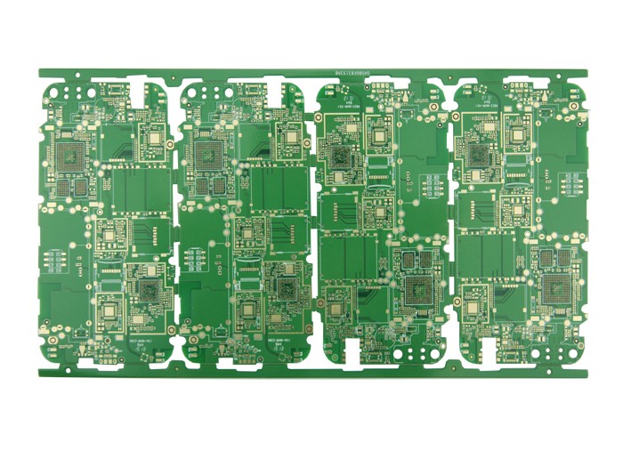
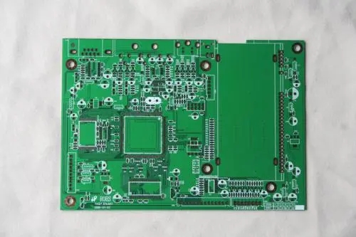
3. Multilayer PCB board
In order to increase the area that can be wired, multi-layer boards use more single or double-sided wiring boards. Use one double-sided as the inner layer, two single-sided as the outer layer, or two double-sided as the inner layer and two single-sided as the outer layer of the printed circuit board. The positioning system and the insulating bonding material alternately together and the conductive pattern Printed circuit boards that are interconnected according to design requirements become four-layer and six-layer printed circuit boards, also known as multilayer PCBs.
PCB board are divided into rigid circuit boards, flexible circuit boards, and rigid-flex boards.
1. The common thickness of rigid PCB is 0.2mm, 0.4mm, 0.6mm, 0.8mm, 1.0mm, 1.2mm, 1.6mm, 2.0mm, etc.
Common materials for rigid PCB include: phenolic paper laminate, epoxy paper laminate, polyester glass mat laminate, epoxy glass cloth laminate, and flexible PCB materials include polyester film, polyimide Amine film, fluorinated ethylene propylene film.
2. The common thickness of flexible PCB is 0.2mm, and the parts to be welded will be added with a thick layer behind it. The thickness of the thick layer varies from 0.2mm to 0.4mm.