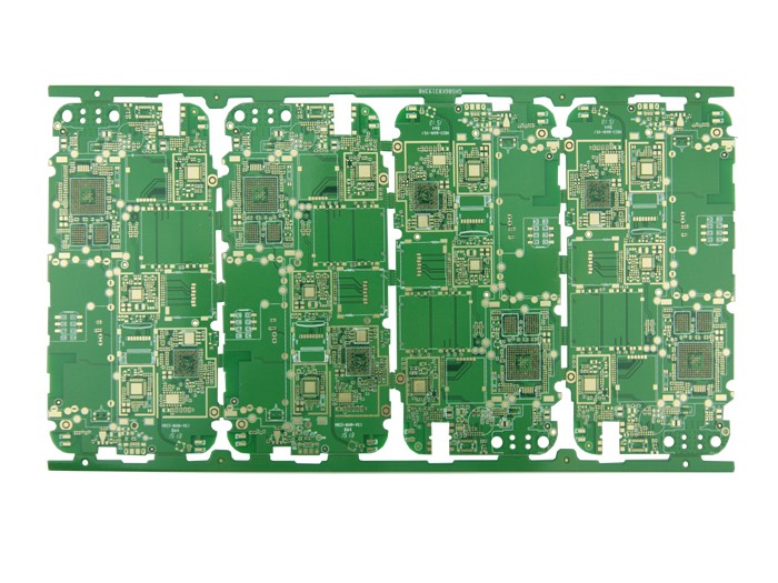
There are generally several reasons for copper paving.

1. EMC. For large-area ground or power supply copper, it will play a shielding role, and some special grounds, such as PGND, play a protective role.
2. PCB board process requirements. Generally, in order to ensure the electroplating effect, or the lamination is not deformed, copper is laid on the PCB layer with less wiring.
3. The signal integrity is required to provide a complete return path for high-frequency digital signals and reduce the wiring of the DC network. Of course, there are also reasons such as heat dissipation, special device installation requires copper and so on.
1. One of the major benefits of copper paving is to reduce the ground wire impedance (a large part of the so-called anti-interference is also caused by the reduction of ground wire impedance). There are a large number of spike currents in digital circuits, so it is more necessary to reduce the ground wire impedance. It is generally believed that a large area of ground should be laid for circuits composed of digital devices, while for analog circuits, the ground loop formed by laying copper will cause electromagnetic coupling interference to outweigh the gains (except for high-frequency circuits). Therefore, it is not that all circuits require ordinary copper (BTW: the performance of mesh copper paving is better than that of a whole block)
2. The significance of circuit copper paving lies in: 1. The copper paving is connected to the ground wire, which can reduce the loop area. 2. The large-area copper paving is equivalent to reducing the resistance of the ground wire and reducing the voltage drop from these two points. In other words, whether it is digital ground or analog ground, copper should be laid to increase the anti-interference ability, and at high frequency, the digital ground and analog ground should be separated to spread copper, and then connected with a single point. This single point can Use a wire to wind a few turns on a magnetic ring, and then connect. However, if the frequency is not too high, or the working conditions of the instrument are not bad, it can be relatively relaxed. The crystal oscillator can be regarded as a high-frequency emission source in the circuit. You can spread copper around and ground the shell of the crystal oscillator, which will be better.
3. What is the difference between a copper block and a grid? To analyze in detail, there are probably three functions:
1. Beautiful appearance 2. Noise suppression 3. In order to reduce high-frequency interference (the reason on the circuit board) According to the routing criterion: the power supply and the ground layer should be as wide as possible, why do we need to add a grid? Ah, isn't it inconsistent with the principle? If you look at it from a high-frequency point of view, it is even more wrong. In high-frequency wiring, sharp traces are taboo. If there are more than 90 degrees in the power layer, there are many problems. In fact, why do it like that is entirely a process requirement: see if the hand-soldered type is painted like that, almost none; if you see such a painting, there must be a chip on it, because there is a kind of craftsmanship when mounting. Called wave soldering, he needs to locally heat the board. If the specific heat coefficients of the two sides are not the same if the copper is spread all over, the board will be up and the problem will arise when the board is up. The pin of the chip is in the upper steel cover (which is also required by the process). It is easy to make mistakes and the scrap rate goes straight up. In fact, this approach has disadvantages: under our current corrosion process: the film is easy to stick to it. In the later strong acid project, that point may not be corroded, and there are a lot of waste products., But only if the board is broken and the chip on it is finished with the board! From this perspective, do you know why you have to paint like that? Of course, some surface mounts are not gridded. From the point of view of product consistency, there may be 2 situations: 1. His corrosion process is very good; 2. He does not use wave soldering but uses More advanced reflow welding, but in this case, the investment of the entire assembly line will be 3-5 times higher.
The above is an introduction to the role of copper in PCB. Ipcb is also provided to PCB manufacturers and PCB manufacturing technology.