Printedcircuit board PCB and parts packaging technology

PCB (Printed Circuie Board) is the abbreviation of printed circuit board, usually on the insulating material, according to the predetermined design, made into the conductive pattern of the printed circuit, the printed element or the combination of the two is called the printed circuit. The conductive pattern that provides electrical connections between components on an insulating substrate is called a printed circuit. In this way, the printed circuit or the finished board of the printed circuit is called a printed circuit board, also called a printed circuit board or a printed circuit board.
There are no parts on the standard PCB, and it is often called "Printed Wiring Board (PWB)".
In order to fix the parts on the PCB, we solder their pins directly on the wiring. On a basic PCB (single panel), the parts are concentrated on one side, and the wires are concentrated on the other side. In this case, we need to make holes in the board so that the pins can pass through the board to the other side, so the pins of the parts are soldered to the other side. Because of this, the front and back sides of the PCB are called Component Side and Solder Side respectively.
If there are certain parts on the PCB that need to be removed or installed back after the production is completed, then the socket will be used when installing the part. Since the socket is directly welded to the board, the parts can be disassembled and assembled at will. Seen below is the ZIF (Zero I ertion Force) socket, which allows parts (here refers to the CPU) to be easily inserted into the socket or removed. The fixing rod next to the socket can be fixed after you insert the part.
If you want to connect two PCBs to each other, generally we will use the edge connector (edge co ector) commonly known as "golden finger". There are many exposed copper pads on the golden fingers, which are actually part of the PCB wiring. Generally, when connecting, we insert the golden fingers on one PCB into the appropriate slot on the other PCB (generally called the expansion slot Slot). In computers, display cards, sound cards, or other similar interface cards are connected to the motherboard by golden fingers.
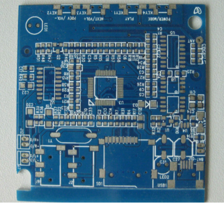
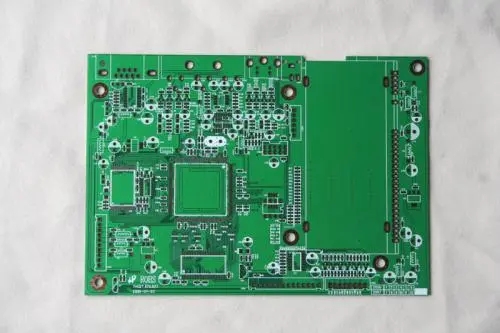
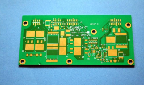
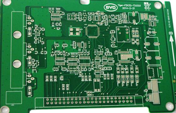
The green or brown on the PCB is the color of the solder mask. This layer is an insulating protective layer, which can protect the copper wire and prevent the parts from being welded to the wrong place. A layer of silk screen will be printed on the solder mask. Usually words and symbols (mostly white) are printed on this to mark the position of each part on the board. The screen printing surface is also called the legend surface.
Single-Sided Boards
We just mentioned that on a basic PCB, the parts are concentrated on one side, and the wires are concentrated on the other side. Because the wires only appear on one side, we call this kind of PCB a single-sided (Single-sided). Because single-sided boards have many strict restrictions on the design of the circuit (because there is only one side, the wiring cannot cross and must be around a separate path), so only early circuits use this type of board.
Double-Sided Boards
This kind of circuit board has wiring on both sides. However, to use wires on both sides, there must be a proper circuit connection between the two sides. This kind of "bridge" between circuits is called a via. A via is a small hole filled or coated with metal on the PCB, which can be connected with the wires on both sides. Because the area of the double-sided board is twice as large as that of the single-sided board, and because the wiring can be interleaved (it can be wound to the other side), it is more suitable for use in circuits that are more complicated than the single-sided board.
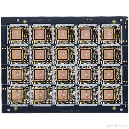
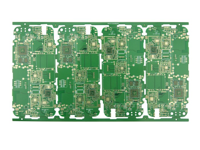
In order to increase the area that can be wired, more single- or double-sided wiring boards are used for multilayer boards. The multi-layer board uses several double-sided boards, and a layer of insulating layer is placed between each board and then glued (press-fitted). The number of layers of the board means that there are several independent wiring layers. Usually the number of layers is even and includes the two outer layers. Most motherboards have 4 to 8 layers of structure, but technically it is possible to achieve nearly 100 layers of PCB boards. Most large supercomputers use fairly multi-layered motherboards, but because these types of computers can already be replaced by clusters of many ordinary computers, super-multilayered boards have gradually ceased to be used. Because the layers in the PCB are tightly integrated, it is generally not easy to see the actual number, but if you look closely at the motherboard, you may be able to see it.
The via we just mentioned, if it is applied to a double-sided board, it must penetrate the entire board. However, in the multilayer board, if you only want to connect some of the lines, the vias may waste some line space in other layers. Buried vias and blind vias technologies can avoid this problem because they only penetrate a few layers. Blind holes are to connect several layers of internal PCB to the surface PCB, without having to penetrate the entire board. Buried vias only connect to the internal PCB, so they cannot be seen from the surface.
In a multilayer PCB, the entire layer is directly connected to the ground wire and the power supply. So we classify each layer as signal layer, power layer or ground layer. If the parts on the PCB require different power supplies, this type of PCB usually has more than two layers of power and wire.
Part packaging technology
Through Hole Technology
Place the parts on one side of the board and solder the pins on the other side. This technology is called "Through Hole Technology (THT)" packaging. This kind of part will take up a lot of space, and a hole must be drilled for each pin. So their pins actually take up space on both sides, and the solder joints are also relatively large. But on the other hand, THT parts are better than smt (Surface Mounted Technology, surface mount technology) parts, and the structure of the PCB board connection is better. We will talk about this later. Sockets like flat cables and similar interfaces need to be able to withstand pressure, so usually they are all THT packages.
Surface Mounted Technology (Surface Mounted Technology)
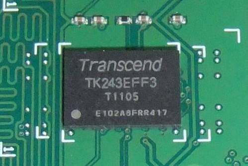
Surface Mounted Technology (smt) parts are used, and the pins are soldered on the same side as the parts. This technique does not need to solder each pin, but drill holes in the PCB.
Surface-mounted parts can even be welded on both sides.
smt is also smaller than THT parts. Compared with PCBs using THT parts, PCBs using smt technology have much denser parts. The smt package parts are also cheaper than THT. So it is not surprising that most of the PCBs today are smt.
Because the solder joints and parts have very small pins, it is very difficult to solder manually. But if you consider that the current assembly is fully automatic, this problem will only occur when repairing parts.