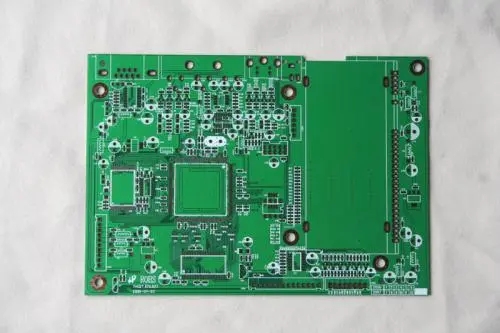
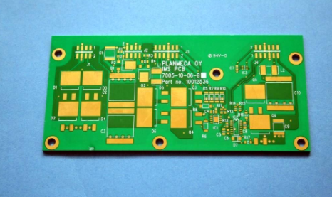
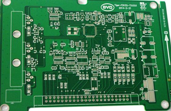
First records the model, parameters, and positions of all vital parts on paper, especially the direction of the diode, the direction of the three-machine tube, and the direction of the IC gap. It is best to use a digital camera to take two photos of the location of the vital parts Photo.
The second step is to remove all the components and remove the tin in the PAD hole. Clean the PCB with alcohol, and then put it into the scanner. When the scanner scans, you need to raise the scanned pixels slightly to get For a clearer image, start POHTOSHOP, scan the silk screen surface in color, save the file and print it out for later use.
The third step is to ligh

tly polish the two layers of TOP LAYER and BOTTOM LAYER with water gauze paper, and polish until the copper film is shiny. Put it in the scanner, start PHOTOSHOP, and scan the two layers in color separately. Note that the PCB must be placed horizontally and straight in the scanner, otherwise the scanned image will be unusable, and the file will be saved.
Step four, Adjust the contrast and brightness of the canvas to make the part with copper film and the part without copper film have a strong contrast, then turn the second image into black and white, check whether the lines are clear, if it is not clear, repeat this step. If it is clear, change The picture is saved as black and white BMP format files TOP.BMP and BOT.BMP, if you find that there is a problem with the picture, you can use PHOTOSHOP to repair and correct it.
The fifth step is to convert the two BMP format files into PROTEL format files, and transfer two layers in PROTEL. For example, the positions of PAD and VIA that have passed through the two layers basically coincide, indicating that the first few steps have been done well, if If there is a deviation, repeat the third step.
Sixth, convert the BMP of the TOP layer to TOP.PCB board, pay attention to the conversion to the SILK layer, which is the yellow layer, and then you can trace the line on the TOP layer, and according to the second Place the device in the drawing of the step. After drawing, delete the SILK layer.
The seventh step, convert the BMP of the BOT layer to BOT.PCB, pay attention to the conversion to the SILK layer, which is the yellow layer, and then you will trace the line on the BOT layer That's it. After drawing, delete the SILK layer.
The eighth step, import TOP.PCB and BOT.PCB in PROTEL, and combine them into one picture. Step ninth, use a laser printer to set TOP LAYER, BOTTOM Print the LAYER on the transparent film separately (1:1 ratio), put the film on the PCB, and compare whether it is wrong, if it is correct, you are done.
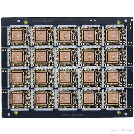
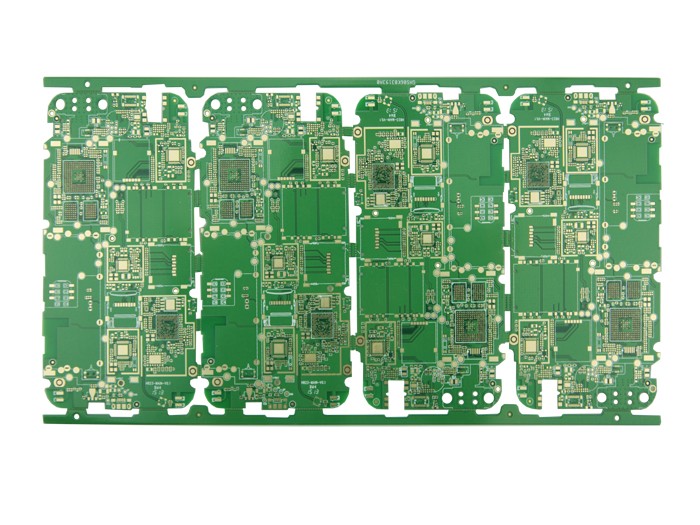
Other: If it is a multilayer board, you need to polish it carefully Go to the inner layer and repeat the third to ninth steps at the same time. Of course, the naming of the graphics is also different. It should be determined according to the number of layers. Generally, double-sided board copying is much simpler than multi-layer board, and multi-layer board copying is easy to appear. In the case of misalignment, the multi-layer board should be particularly careful and careful when copying the board (the internal vias and non-vias are prone to problems).