The design quality of PCB proofing printed circuit boards not only directly affects the reliability of electronic products, but also relates to the stability of the products, and even the key to the success or failure of the design. Therefore, when designing a printed board diagram, in addition to providing correct electrical connections for the components in the circuit, the anti-interference of the printed board should also be fully considered. Based on the principle of electromagnetic compatibility, anti-interference design should include three aspects: one is to suppress the noise source, the other is to cut off the noise transmission path, and the third is to reduce the noise sensitivity of the disturbed device. The noise suppression of the printed board should start from the design stage and run through a series of links such as circuit schematic design, printed board drawing, component selection, and printed board mounting leads. Although the focus of each link is different, but they echo each other, they should all be taken seriously. This article mainly introduces how to effectively suppress noise when designing printed boards. Reduce radiated noise The printed circuit board will radiate noise outwards and become a noise source when it is working: the signal line in the circuit board is transmitted to the chassis through the ground loop, causing resonance, and strong noise is radiated from the chassis; the signal of the circuit board passes through the signal The cable radiates noise outward; the circuit board itself also radiates noise directly. In order to weaken the noise radiation, the following treatments can be done:

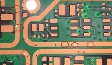
(1) Select the device carefully. When selecting, pay attention to the aging of components, and select components with less thermal feedback. For high-frequency circuits, suitable chips should be selected to reduce circuit radiation. When choosing a logic device, it is necessary to fully consider its noise tolerance index: When the noise tolerance of the circuit is simply considered, it is best to use HTL. If power consumption is considered, CMOS with VDD≥15V is appropriate.(2) Use multilayer printed circuit boards. In this way, the ideal shielding effect can be obtained from the structure: use the middle layer as the power line or the ground line, seal the power line in the board, and do insulation treatment on both sides, so that the switching currents flowing through the upper and lower sides will not affect each other; printed board The inner layer is made into a large-area conductive area, and there is a large electrostatic capacitance between each wire surface, forming a power supply line with extremely low impedance, which can effectively prevent the circuit board from radiating and receiving noise.(3) The printed circuit board is "fully grounded". When drawing a high-frequency circuit board, in addition to thickening the grounding printed wire as much as possible, all the unoccupied area of the circuit board should be used as a grounding wire, so that the device can be better grounded nearby. This can effectively reduce the parasitic inductance, and at the same time, the large-area ground wire can effectively reduce noise radiation. (4) One or two grounding plates are attached to the printed circuit board. That is, an aluminum sheet or iron sheet is attached to the back of the printed board (welding surface), or the printed board is sandwiched between two aluminum or iron plates. When installing the grounding board as close as possible to the printed board, and be sure to connect it to the best grounding point of the system signal (SG). This structure is essentially a simple and easy-to-make "multi-layer" printed board. If you want to pursue a better suppression effect, you can install the printed board in a completely shielded metal box, so that it does not generate or respond to noise. Properly lay out the printed wires. Wiring is the key stage of the graphic design of the printed circuit board. Many factors considered in the design should be reflected in the wiring, such as the layout of the copper foil wires on the printed board and the crosstalk between adjacent wires. It will determine the immunity of the printed board, and reasonable wiring can make the printed board obtain the best performance. From the perspective of anti-interference, the design and process principles that should be followed for wiring are: (1) As long as the wiring requirements are met, single-sided boards should be selected first, followed by double-sided boards and multilayer boards. The wiring density should be reasonably selected based on the structure and electrical performance requirements, and strive to be simple and uniform; the minimum width and spacing of the wires should generally not be less than 0.2mm. When the wiring density allows, the printed wires and their spacing should be appropriately widened. (2) The main signal lines in the circuit should best be gathered in the center of the board, and try to be close to the ground wire, or surround it with the ground wire. The loop area formed by the signal wire and the signal loop wire should be the smallest; try to avoid long-distance parallel wiring, The wiring between the electrical interconnection points in the circuit strives to be the shortest; the corners of the signal (especially high-frequency signal) lines should be designed to be 135°, or circular or arc, and do not draw 90° or less. (3) Adjacent wiring surface conductors take the form of mutually perpendicular, oblique or curved wiring to reduce parasitic coupling; high-frequency signal conductors must not be parallel to each other to avoid signal feedback or crosstalk, and additional installations can be made between two parallel lines A ground wire.(4) Properly route the external signal lines, shorten the input lead as much as possible, and increase the impedance of the input end. It is best to shield the analog signal input line. When there are analog and digital signals on the board at the same time, it is advisable to isolate the ground wires of the two to avoid mutual interference.(5) Properly handle redundant input terminals of logic devices. Connect the redundant input terminal of the NAND gate to "1" (don't leave it floating), or connect the redundant input terminal of the NOR gate to Vss, and connect the idle set/reset terminals of counters, registers and D flip-flops to Vcc via appropriate resistors to trigger The redundant input terminal of the device must be grounded.(6) Choose standard component package. When you need to create a component package, the pad hole pitch should be the same as the device pin pitch to reduce lead impedance and parasitic inductance. When laying wires, metallized vias should be minimized to improve the reliability of the entire printed board.